Incheol (Aiden) Jung: received the B.S. and M.S. degrees in physics from Inha University, Incheon, South Korea, in 2021 and 2023, respectively, where he delved into optics, nanophotonics, and inverse design. He is currently pursuing the Ph.D. degree in electrical and computer engineering at University of Illinois at Urbana-Champaign, Urbana, IL, USA. His research interest spans to electromagnetic wave physics, inverse design, material homogenization, and computational electromagnetics. (Email: incheol3@illinois.edu)
Zhen Peng: received the B.S. degree in electrical engineering and information science from the University of Science and Technology of China, Hefei, China, in 2003 and the Ph.D. degree in electromagnetics and microwave engineering from Chinese Academy of Science, Beijing, China, in 2008. From 2008 to 2013, He was with the ElectroScience Laboratory, The Ohio State University, Columbus, OH, USA, first as a Post-Doctoral Fellow (2008–2009) and then as a Senior Research Associate (2010–2013). From 2013 to 2019, He was an Assistant Professor at Department of Electrical and Computer Engineering, The University of New Mexico (UNM), Albuquerque, NM, USA. He is currently an Associate Professor at Department of Electrical and Computer Engineering (ECE ILLINOIS), University of Illinois at Urbana-Champaign, Champaign, IL, USA. His research interests are in the areas of computational, statistical, and applied electromagnetics. The goal is to simulate classical and quantum electrodynamic physics with intelligent algorithms on state-of-the-art computers, where virtual experiments can be performed for the prediction, discovery, and design of complex systems at unprecedented scales. His research work has an impact on both civilian and commercial engineering applications, including advanced antennas, radio frequency integrated circuits, electromagnetic interference and compatibility, signal and power integrity, and wireless communication. Dr. Peng is a recipient of the 2022 16th European Conference on Antennas and Propagation Best Electromagnetics Paper Award, 2021 30th Conference on Electrical Performance of Electronic Packaging and Systems (EPEPS) Best Conference Paper Award, 2019 IEEE Electromagnetic Compatibility Symposium Best Paper Award, 2019 EPEPS Best Conference Paper Award, 2018 National Science Foundation CAREER Award, 2018 Best Transaction Paper Award-IEEE Transactions on Components, Packaging and Manufacturing Technology, 2017 IEEE Albuquerque Section Outstanding Young Engineer Award, 2016 UNM Electrical and Computer Engineering Department’s Distinguished Researcher Award, 2015 Applied Computational Electromagnetics Society Early Career Award, 2014 IEEE Antenna and Propagation Sergei A. Schelkunoff Transactions Prize Paper Award, multiple Young Scientist Awards and the advisor of 12 Best Student Paper Awards to date from various conferences. (Email: zvpeng@illinois.edu)
Yahya Rahmat-Samii: is a Distinguished Professor and holder of the Northrop-Grumman Chair in electromagnetics at Department of Electrical and Computer Engineering (ECE), University of California, Los Angeles (UCLA), CA, USA. He is a member of the U.S. National Academy of Engineering (NAE), a Foreign Member of Chinese Academy of Engineering (CAE), and Royal Flemish Academy of Belgium for Science and the Arts. He is the recipient of the 2011 IEEE Electromagnetics Field Award and formerly served as Chairman of ECE Department at UCLA and as a Senior Research Scientist at Caltech/NASA’s Jet Propulsion Laboratory. He served as the President of the IEEE Antennas and Propagation Society (AP-S) in 1995 and as President of United States National Committee (USNC) of the International Union of Radio Science (URSI) from 2009 to 2011. He has also served as an IEEE Distinguished Lecturer, delivering lectures internationally. He has authored or coauthored over 1100 technical journal and conference papers, along with more than 40 book chapters and seven books. His work has been featured on the cover of over 20 IEEE publications. His research encompasses various areas of modern electromagnetics and antennas, ranging from small medical antennas to large space deployable antennas. His interests include electromagnetics, antennas, measurement and diagnostic techniques, numerical and asymptotic methods, satellite and personal communications, human/antenna interactions and medical applications, meta-materials and periodic structures, as well as nature-inspired optimization algorithms. Dr. Rahmat-Samii is a Life Fellow of IEEE, Antenna Measurement Techniques Association (AMTA), Applied Computational Electromagnetics Society (ACES), Electromagnetics Academy (EMA), and URSI. He received the Henry Booker Award from URSI in 1984, which is given triennially to the most outstanding young radio scientist in North America. Additionally, he was awarded the Best Application Paper Prize (Wheeler Award) of IEEE Transactions on Antennas and Propagation in 1992 and 1995, The University of Illinois ECE Distinguished Alumni Award in 1999, the IEEE Third Millennium Medal, and the AMTA Distinguished Achievement Award in 2000. In 2001, he received an Honorary Doctorate Causa from University of Santiago de Compostela, Spain. Further accolades include the 2002 Technical Excellence Award from JPL, the 2005 URSI Booker Gold Medal presented at the URSI General Assembly, the 2007 IEEE Chen-To Tai Distinguished Educator Award, and the 2009 Distinguished Achievement Award of the IEEE AP-S. He also received the 2010 UCLA School of Engineering Lockheed Martin Excellence in Teaching Award and the 2011 Campus-Wide UCLA Distinguished Teaching Award. Dr. Rahmat-Samii was honored with the Distinguished Engineering Educator Award from The Engineers Council in 2015, the John Kraus Antenna Award of the IEEE AP-S, and the NASA Group Achievement Award in 2016. In 2016, he received the ACES Computational Electromagnetics Award and the IEEE AP-S S. A. Schelkunoff Best Transactions Prize Paper Award. He was awarded the prestigious Ellis Island Medal of Honor in 2019, which is given annually to distinguished U.S. citizens who exemplify a life dedicated to community service. These individuals preserve and celebrate the history, traditions, and values of their ancestry while embodying the values of the American way of life and striving to create a better world. In 2020, he received the AIAA (American Institute of Aeronautics and Astronautics) Best Paper Award, followed by the 2022 IEEE AP-S Harrington-Mittra Award in Computational Electromagnetics. In 2023, he was honored with the National Academy of Sciences USNC-URSI Outstanding Educator Award and the IEEE AP-S Outstanding Service Award. He designed the original logo for the IEEE AP-S, displayed on all IEEE AP-S publications. In 2023, he was designated as “Legend of Electromagnetics” by the IEEE AP-S, with his interview available at: https://www.youtube.com/watch?v=HO2-nrC2rCM. (Email: rahmat@ee.ucla.edu)
This paper presents a comprehensive review of recent advances in reconfigurable electromagnetic (EM) surfaces. The discussion is organized around three key aspects of reconfigurable EM surfaces: unit cell engineering design, full-wave numerical analysis, and large-scale optimization techniques. Numerous references are provided to facilitate further exploration of this compelling and timely subject. To address the above three key aspects, we conduct an extensive examination of the design process for metasurfaces in reconfigurable devices. This involves evaluating the design methodology of unit cells, EM simulation techniques tailored for highly complex structures, and innovative optimization methods suitable for scenarios with numerous variables. In scenarios featuring reconfigurability for real-time manipulation of EM waves to meet the requirements of emerging communication environments, the optimization cost function is defined with multiple variables, exhibiting intricate behavior in the design space. Consequently, it necessitates an optimization methodology capable of handling high-dimensional functions without getting trapped in local minima. Moreover, the intricate geometries of metasurface devices preclude analytical solutions, necessitating high-performance full-wave solvers capable of providing highly accurate simulations with minimal computational expense. Key concepts and details pertaining to the aforementioned design stages are presented in a unified manner, along with representative examples.
Over the past two decades, metamaterials and metasurfaces have received significant attention in the scientific and engineering community due to their unique electromagnetic (EM) and optical properties [1]-[8]. They offer a range of versatile and exceptional responses that are not readily available in nature. The first generation of metamaterials is made by volume arrangements of microscopic structures. Since the EM response of metamaterials can be readily modified by morphing the unit cell structure unlike in the real materials, a high variety of material properties can be achieved, yielding negative refraction, negative permittivity and permeability, and bi-anisotropic parameters.
Despite the promising potential of metamaterials, devising the unit cell for three-dimensional (3D) structures can be intractably involved. Hence, a significant amount of attention is given to metasurfaces [8]-[11], which are the two-dimensional (2D) counterpart of metamaterials. The reduced dimensionality mitigates complexity in both design and fabrication, thereby allowing the use of highly complex unit cells which enable the realization of a wider variety of material properties. The increased versatility advocates for devices harnessing metasurfaces to exhibit high performance in various areas with compact designs. For example, an optical lens system, which needs to be bulky to offer the wavefront shaping of the incident wave, can be suppressed into flat surfaces utilizing metasurfaces [12]-[14]. Also, metasurfaces can be incorporated to mitigate the inevitable aberration, especially for compact optical systems [15].
Today, the field of EM surface research and development is fast evolving. We have witnessed the evolution of structures, progressing from periodic to quasi-periodic to aperiodic arrays, aiming for advanced control over parameters such as amplitude, phase, and polarization, as well as advanced manipulation of plane/radiated waves and surface/guided waves. Particularly, we have seen a rapidly increased study of reconfigurable EM surfaces, also known as tunable metasurface or programmable EM surfaces. Unit cells in reconfigurable devices demonstrate the capability to transition between multiple states, facilitating functionalities such as beamforming, wave-front shaping, and phase modulation. This enhanced flexibility in modulation empowers the EM surface with greater versatility and functionality.
One well-known example is the reconfigurable intelligent surfaces (RISs) that can modulate the incident EM wave towards the user locations with high directivity thus enhancing the power efficiency. Moreover, the EM modulation can be performed not only on a single beam but also on multiple beams such that they are highly applicable to multi-user multi-input multi-output (MIMO) allowing the user detection, signal processing, and optimized resource allocation for 6G wireless communication networks.
The reconfigurability in EM surfaces can be achieved with various tunable loaded structures such as diodes [16], microelectromechanical systems (MEMS) [17], varactors [18], and liquid crystals (LCs) [19]. For instance, some studies employ LCs to create reconfigurability, taking advantage of their anisotropic property [20]. With different voltage application, the molecules rotates thus causing a change of permittivity to the direction of interest. The change of the permittivity of LC creates different phase shifts in the device, leading to tunability of the resonant frequency. For another example, electric switching components such as p-i-n diodes can be utilized to control the reconfigurable surfaces [21]. By turning on/off the switch, the current profile on each unit cell evolves affecting the EM response of the total EM surface. More detailed descriptions and the discussion regarding the methods will be presented in Section II.
This domain of research leads to many new functionalities and applications, including reconfigurable beamshaping [22], switch-reconfigured antennas [23], energy selective surfaces [24], waveform-dependent absorbing metasurfaces [25], [26], and power-dependent impedance surfaces [27]-[29], reprogrammable imaging [30], diffractive neural networks [8], [31], [32], and RISs in mobile communication systems [33]-[36]. An overview of the EM metasurfaces research is recently summarized in [37] and [38] and special issues [39], [40].
In this paper, we present a review of recent advances in reconfigurable EM surfaces. The discussion is structured around three fundamental aspects of reconfigurable EM surfaces: unit cell engineering design, full-wave numerical analysis, and large-scale optimization techniques.
The initial stage of EM surface design involves engineering the unit cell, a foundational process that integrates established theories with engineering insight. We will first explore analytical approaches, followed by numerical models that homogenize the unit cell’s subwavelength structure to extract its effective electromagnetic properties. Based on the predicted effective properties, unit cells can be designed to achieve the desired electromagnetic properties for optimizing the functionality of the metasurface. Our emphasis then shifts to the switch-reconfigured unit cell, enabling low-cost beam-steerable reflectarrays, transmitarrays, and RISs. With reconfigurability introduced, EM devices can actively modulate their response to efficiently allocate resources, thereby enhancing wireless communication for smart radio environments.
The succeeding step involves verifying the EM device’s performance through numerical solutions of Maxwell’s equations. While theoretical analyses of metasurface unit cells provide insights into EM responses, achieving higher accuracy necessitates full-wave simulations, especially for complex structures. We will introduce and elaborate on an efficient full-wave numerical framework built upon the hybrid finite element (FE)-boundary integral (BI) equation formulation. This method combines the strengths of both FE and BI techniques to offer a versatile and accurate approach for analyzing electromagnetic structures across various scenarios.
Finally, numerical optimization plays a crucial role in the design of EM surfaces. When combined with a full-wave solver, optimization algorithms can adjust the design parameters to achieve high performance. For simpler structures like passive metasurfaces, an initial design can often be obtained using an analytical approach and then refined using optimization tools. This refinement is necessary because initial designs may be sub-optimized due to simplifications made for mathematical convenience, leading to the omission of certain EM effects during the unit cell design process. By incorporating a full-wave solver, which can capture inaccuracies in the initial calculations, further optimization becomes achievable through fine-tuning.
On the other hand, complex devices like reconfigurable EM surfaces pose challenges due to their high complexity and large number of variables, which can overwhelm human designers. Thus, numerical optimization techniques become essential from the beginning of the design process. This approach, often termed inverse design, involves computationally optimizing both geometrical and material parameters. In an inverse design framework, designers parameterize geometry and materials, enabling optimization algorithms to be applied. Alternatively, topology optimization can be utilized, where unit cell geometry is automatically generated. Unlike conventional approaches that parameterize geometry, topology optimization assigns variables to materials at each pixel of the discretized geometry, hence facilitating the optimization of arbitrary geometries [41]-[43].
II.
Engineering Unit Cells
1
Motivation
From a molecular perspective, EM material properties like permittivity, permeability, and conductivity can be understood from the interactions between molecules when subjected to an alternating current (AC) in the form of an EM wave. Depending on the binding energy of the electrons, the material can be conceptualized as either a collection of dipoles or a continuous volume through which free electrons move [44], [45]. These electromagnetic behaviors at the microscale ultimately manifest as material properties at the macroscale [46].
The advantage of artificial molecules lies in the reduced constraints on geometry formation and material selection, resulting in a broader spectrum of material properties compared to those found in natural materials. Leveraging these artificial properties, EM devices can exert greater control over EM waves, enabling the realization of exotic functionalities such as superdirectivity [22], wavefront shaping [14], [47], anomalous reflection or transmission [48], [49], and leaky-wave mode transition [50]. Moreover, by introducing switching capabilities to the unit cell, reconfigurable properties can be imparted to the devices, enabling the realization of tunable EM devices. The modulation of EM properties can be achieved continuously by gradually changing the geometry or material properties of the unit cells [51]-[53]. However, for practical applications, unit cells are usually designed to switch between a limited number of states, resulting in quantized states of reconfigurable unit cells.
Reviewing all these interesting surfaces and their development, two prominent features emerge. The first is the discretization of the surface from a continuous state to a discrete array, aiming to enable localized and distributed wave control. According to Nyquist’s sampling principle, a continuous function can be discretized into a series of data with a proper sampling rate, maintaining information integrity. In surface EM, when the surface is discretized with a spacing smaller than half the wavelength, the discrete surface can exhibit the same spectral performance as the corresponding continuous surface. The discretization process transforms the surface into a periodic lattice, where each element can be uniform (resulting in a periodic surface) or varied (resulting in a quasi-periodic surface). Nonetheless, discretization empowers each element to manipulate EM waves locally and individually. Though interactions between adjacent elements may persist, they can be controlled or minimized. These individual elements are then arranged on the surface with various distributions such as uniform, gradient, or hologram distribution. Consequently, the cumulative effect of all individual wave controls manipulates the wavefront as desired, facilitating actions like a mirror reflection, anomalous reflection, or reflection with a specifically focused beam.
The second prominent feature of advanced EM surfaces is the capability to comprehensively control EM waves. Early surface designs focused solely on specific aspects of the wave, such as magnitude, phase, or polarization. However, recent advancements require simultaneous control over magnitude, phase, and polarization. Furthermore, researchers are increasingly interested in anisotropic surfaces with tensor characteristics and non-dispersive surfaces with wide bandwidth. Non-linear and non-reciprocal surfaces have also emerged in the literature. Additionally, advanced surfaces integrating real-time control through the integration of circuit components are of great interest to both researchers and engineers. This integration combines spatial variation through the surface with time variation through the circuit. It is believed that the capability of surfaces to control EM waves will continue to grow in power with the development of surface electromagnetics.
This section aims to present the unit cell design process. The discussion starts with analytical models that forecast the effective material properties of subwavelength structures. These models progress from volumetric to surface representations, extracting equivalent surface impedance. Building on these features, unit cells can be regarded as homogeneous pixels, with material properties customized to attain the desired functionality. Subsequently, methods for incorporating reconfigurability into unit cells are introduced. Additionally, this section discusses the device physics that facilitates reconfigurability and investigates their potential in tackling real-world challenges.
2
From volumetric to surface properties
To analyze the EM behavior of mixed medium, effective medium theory can be employed. In this classical mixing model, for the convenience of mathematics, the geometry is required to be in a subwavelength scale, sufficing quasi-static condition where the geometry is sufficiently small that the EM wave can be approximated as a uniform field. As shown in Figure 1, with the applied field, the charges are depolarized creating the internal depolarized field \boldsymbol{E}. Therefore, the total field \boldsymbol{E}_0 is described as the subtraction from the applied field \boldsymbol{E}_a to the depolarized field.
Figure
1.
A schematic view of the geometry that is considered in the effective medium model. Under the quasi-static condition, a uniform field is applied to the inclusion incurring the charges to be depolarized. \epsilon_h and \epsilon_i respectively refer to the permittivities of the host and inclusion media.
Utilizing the total field to calculate the effective flux in the homogenized biphasic material, the effective permittivity can be evaluated. Representatively, by following the Bragg-Pippard approach [54], {\boldsymbol{E}}_d can be calculated for various inclusion shapes by employing the depolarization factor which parameterizes the depolarization behavior of the charges in the inclusion geometry [55]. From the calculated total field, effective susceptibility can be obtained, thus resulting in the effective permittivity [54]:
where {\cal{F}} stands for the volume fraction, Q refers to the depolarization factor, and \chi_\text{eff} and \chi symbolize the effective and the inclusion’s electric susceptibilities, respectively. Since \chi_\text{eff} and \chi are by definition:
where \epsilon_i , \epsilon_h , and \epsilon_\text{eff} represent the permittivities of the inclusion, host, and equivalent media, respectively, the effective permittivity can be expressed as
The effective permeability can also be evaluated with the same strategy utilizing the magnetic properties instead of the electric properties according to the EM duality. Moreover, this approach can be exploited for each axis of the mixed medium, so that the anisotropy can be considered. Furthermore, the models are extended to the wider applicable regime that encompasses larger inclusion scales that violate the quasi-static condition [56], or higher geometrical complexity such as core-shell cylinders [57].
To achieve an efficient design approach for metasurfaces, a comparable method is utilized in formulating the generalized sheet transition condition (GSTC). This condition delineates the boundary condition for the effective surface properties of metasurface unit cells, such as characteristic impedance or admittance [10], [58]. Considering a disk with a radius of R, the applied electric and magnetic fields ( {{H}} ) can be decomposed similarly to (1), where {{E}}_d and {{H}}_d denote the electric and magnetic depolarizations in the disk, and {{E}}_0 and {{H}}_0 satisfy the classical boundary condition:
where \omega symbolizes the angular frequency, \mu denotes the permeability, {\cal{P}}_s and {\cal{M}}_s refer to the electric and magnetic surface polarization densities, and the subscripts t and {\textit{z}} indicate the field to be tangential and normal to the surface of the disk, respectively. On the other hand, the depolarized fields \boldsymbol{E} _d and \boldsymbol{H}_d are expressed as functions of the electric and magnetic potentials \boldsymbol{F} and \boldsymbol{A} .
The potentials can be calculated by solving Helmholtz equations for the electric and magnetic waves [58]. Substituting the potentials into (7) and (8), and then taking the average of the fields in the disk, the fields are described as
where the superscript {\rm{av}} indicates the averaged field and k={\omega}/{\lambda} stands for the free-space wavenumber. For the complete structure, the polarization density can be described as the sum of the individual polarization density of each inclusion.
where the subscripts ES and MS indicate that the surface susceptibility dyadics relate to the electric and magnetic fields, respectively. Substituting (9) into (1) and then into (10) and (11), the electric and magnetic susceptibility tensors are obtained, which leads to the electric and magnetic polarization densities. The boundary condition of (6) is rewritten as
Utilizing the mixing model and the GSTC as the basic tools, the EM properties of the unit cells can be examined. Also, more complex EM behaviors such as self-resonance, surface wave, and coupling effect can contribute in the unit cell responses. For instance, some unit cell designs simultaneously satisfy both the standing wave and the excitation conditions of plasmon wave, a form of surface EM waves, confining the incident EM energy in a small volume [59], [60]. The effect of the field concentration can provide diverse applications such as filtering [61], sensing [62], [63], and lithography [64].
In recent years, researchers have begun leveraging the unit cell coupling in the EM surface design. Firstly, the coupling effect can be ascribed to the interaction between the charge oscillations in adjacent cells [65], [66]. Numerical studies reveal the dependence of effective permittivity and permeability on the shape and distance between unit cells. The dipole moments created by charge oscillation are reinforced by adjacent cells, akin to cascading capacitors, amplifying with smaller distances and larger adjacent areas. This reinforced dipole moment mimics the smaller depolarization factor in Bragg-Pippard model, resulting in increased effective permittivity. Using this strategy, metasurfaces with exceptionally high permittivity have been engineered.
In [67], a hexagonal unit cell is proposed for a metasurface antenna to improve the bandwidth of radiation. Compared to the square unit cells, the edge of the hexagonal ones supports the surface current flowing through a smoother path which leads to less change in the impedance for different frequencies, as visualized in Figure 2. Moreover, the hexagonal shape, as opposed to a circular shape with even smoother edges, maintains a constant cell distance, resulting in a coherent capacitance-like behavior between cells. With the varying spacing creating variation in the depolarization factor, the circular unit cells attain the narrowest bandwidth despite their edge shape advocating the smoothest current path. Resultingly, the hexagonal shape is selected as the unit cell shape, owing to its smooth shape as well as the constant spacing both of which contribute to the broadband radiation.
Figure
2.
A graphical view of the magnetic field distribution as the reaction to a variety of frequencies of hexagonal geometry of the metasurface [67]. Owing to the shape of the unit cells, the field behavior is less discontinuous at the interfaces, thereby maintaining smooth transition between frequencies so that the EM response is constant over the broadband.
Alternatively, another methodology may be introduced to cope with the coupling effect. In [68], it is explained that the scattered field from each unit cell affects the current density in the other cells thus causing the coupling effect. Therefore, the surface impedance of the unit cell is decomposed into the self-impedance term and the coupling term, and then the EM behavior is analyzed in the method of moments (MoM) formalism. Since each unit cell has its scattering field which affects one another, the localized electric field at p th element can be described as
where the superscripts p and q indicate the p th and q th elements, the superscript s denotes the self-impedance term, V and I represent the voltage and the current, Z refers to the impedance, and J symbolizes the induced current density which is obtained by a full-wave solver such as finite element method (FEM). Equation (12) implies that the localized electric field (Eloc) will be realized by the impedance pattern at the right-hand-side (RHS) of the equation. Therefore, the impedance pattern is materialized as the unit cell design at the p th element. The elementary scattering pattern is computed by utilizing FEM and then compared to that expected from a homogeneous cell with the equivalent impedance:
\begin{array}{*{20}{l}} L = \text{MSE}(Z^{qp}_{q \neq p}(I^p_\text{FEM}-I^p_{H})) + \text{MSE}(E^{p,\text{near}}_\text{FEM}-E^{p,\text{near}}_{H}) \end{array}
(13)
where the superscript \text{FEM} indicates computation by FEM, \text{MSE} denotes mean squared error, and L stands for the loss function which is minimized to attain the optimal unit cell design. I^p_{H} and E^{p,\text{near}}_{H} are analytically calculated from the MoM matrix and by using 2D Green’s function, respectively, under the consideration of the pixelated metasurface with homogeneous unit cells. Employing this strategy, the authors demonstrated metasurface designs materializing wide-angle reflection and beam collimation.
Anisotropic cells can also be devised based on the mixing model [69]. In the work, a square with two cut corners is adopted as the unit cell geometry for a reflective metasurface creating polarization conversion. Unlike the isotropic hexagonal unit cell design discussed previously, the cell proposed here is elongated in the diagonal direction and the spacing between them is asymmetric, endowing anisotropy to the metasurface. Due to the anisotropy, phase retardation occurs between x- and y-polarized reflections, converting the polarization of the incident wave. The metasurface device achieved nearly 90% polarization conversion efficiency over the frequency range from 8 GHz to 12 GHz, under the benefit of the high reflection of the metallic unit cell.
When dielectrics are utilized for unit cells, surface reflections may introduce additional losses. To mitigate these reflections, nano-fin structures have been proposed, implementing a permittivity that simultaneously satisfies quarter-wavelength plate and anti-reflection conditions [70]. These structures feature dimensions of 100 nm in width, 300 nm in length, and a 45° tilt on a 330 nm \times 330 nm unit cell. Parametric sweeps are conducted for height and material to investigate the reflection and power conversion efficiency (PCE) of the device, aiming to identify optimal parameters. The final design comprising \text{MgF}_2 on \text{Nb}_2\text{O}_3 , with respective heights of 140 nm and 950 nm, achieved a total PCE of up to 96%.
Machine learning is another popular strategy for devising unit cells of metamaterials and metasurfaces [71]-[73]. In [74], a tandem network architecture is utilized to obtain the optimal design parameters. The networks can be subdivided into two parts: forward network (FN) and inverse network (IN), where the former provides the prediction of the EM spectral response of the device, and the latter generates design parameters from the given spectral data. They are connected by the design parameters and the spectral data at the input and the output of the entire networks, resembling the structure of the variational autoencoder (VAE). For the input spectra, the algorithm creates design parameters from which it regenerates the predicted spectrum to compare with the input values. The loss is defined as the mean absolute error (MAE).
The FN is pre-trained to accurately predict the EM property of the given design and is used as a surrogate model providing the EM response with greatly reduced computation load compared to that required by full-wave solvers. Subsequently, the IN is trained to generate design parameters for the unit cell to achieve high performance of interest. To apply this design approach, the geometrical parameters of the unit cell [75], such as the size of the unit cell, the radius of the pattern, and the width of the pattern, is linked to the output of the IN, and simultaneously the input of the FN. The neural-network-based method successfully attained high transmittance in the device, outperforming that proposed in the precedent work [74], [75].
Bayesian optimization [76] is becoming another popular strategy in designing complicated unit cells, owing to its advantage of the reduced requirement of the number of simulations. In [77], the authors aim to simultaneously enhance Faraday rotation and transmission in the metasurface structure. To parameterize the arbitrary geometry of the scatterer, the unit cell x - y plane is angularly subdivided to make spoke-patterned lines, on which points \boldsymbol{R} lie within the radial range between R_{\rm{min}} and R_{\rm{max}} so that the points are constrained inside the unit cell area. A periodic centripetal Catmull-Rom spline curve is then generated following the trajectory of the points, forming the outline of the scatterer.
To simultaneously consider both the Faraday rotation and transmittance of the EM surface, a merit function is devised as [77]
where \lambda indicates the wavelength and the \theta and T denote Faraday rotation and transmittance of the EM surface obtained from the simulation using discontinuous Galerkin time-domain (DGTD) solver.
The Bayesian optimization algorithm iteratively selects sample points which achieve the highest potential of maximizing the merit function, employing the expected improvement strategy [76]. Within 10 iterations, the algorithm yielded a star-shaped scatterer design which significantly outperforms the cylindrical scatterer which is used as the reference design. Compared to −10.1° of Faraday rotation and unitary transmittance of the reference one, the optimized design attained −15.2° and 0.96 of Faraday rotation and transmission, attaining 14.9° in the merit function, which is significantly enhanced from that of the reference design, 10.1°.
3
From passive to reconfigurable surface
Artificial unit cells can be enhanced with reconfigurability. Various methods have been proposed to actively modulate the effective material property of these cells, including the use of LC [51], polarization change [78], [79], chemical reactions [53], thermal reactions [52], varactors [80], and electric switches [18], [81]. Through these approaches, manipulations can be applied to either the material property or the geometry of the unit cell component, resulting in a shift in the equivalent property of the cell.
For example, the chemical reaction of LC can be exploited to the unit cell design such that the EM surface displays different images depending on the existence of specific gas [82]. The device consists of a holographic metasurface and an LC layer. The LC layer is initially in the nematic phase, which implies that the molecules are inclined to be aligned in a specific direction. When the layer is exposed to volatile gas, the gas molecules diffuse into the layer disturbing the order of the LC molecules, therefore causing the phase transition to the isotropic phase wherein the LC molecules are in random orientation distribution. Additionally, the layer is designed to be a full-wavelength plate (FWP) in the initial state and a half-wavelength plate (HWP) in the exposed state. When the layer is in FWP mode, the phase retardation is equivalent to a wavelength, maintaining the polarization state of the incident wave. Moreover, in HWP mode wherein the phase retardation is a half wavelength, the polarization evolves to its orthogonal counterpart. For instance, for the polarization of incidence being right-hand circular polarization (RHCP), the transmitted wave from the layer in HWP mode exhibits left-hand circular polarization (LHCP). When it comes to the holographic metasurface, it is engineered to display different holographic images for each polarization of RHCP and LHCP. Since the incident wave has different polarization depending on the existence of the volatile gas, the metasurface device performs as a gas detector.
In addition, the dynamic self-assembly behavior of silver nanoparticles depending on the temperature can be employed for a reconfigurable metamaterial [83]. Based on the heat-dependent self-assembly behaviors of LC coated nanoparticles [84], the state of the particle system switches between the regular and random states as the temperature changes from 30 °C to 120 °C. The different configuration of the particles exhibits different effective material properties of the metamaterial, creating change in the EM response of the device.
Although these implementations successfully introduce tunability to the metasurface devices, their application is somewhat limited due to passive and slow reconfiguration processes. In the rapidly evolving landscape of smart radio environments [85], there is a growing demand for EM surface devices, such as RISs and reconfigurable directive antennas, to exhibit short response times and precise controllability. Electric tunability emerges as a promising solution to meet these requirements effectively.
One valid method of materializing the electric tunability is the utilization of varactors [80]. The change of the reversely biased voltage to the varactor causes the variation in the capacitance, which leads to the evolution of the resonant frequency. The dependency of the resonance in the varactor then creates the controllable reflectance phase shift from the device. When the varactors are assembled as an array, the array can function as an RIS where the angle of reflectance is modulated by the bias. The device harnesses active reconfigurability for beam scanning as well as frequency agility.
Another approach is the use of electric switches such as p-i-n diodes. In [21], a spiral unit cell with three arms connected by p-i-n diodes is presented. As illustrated in Figure 3, the device has three states depending on the activation of one of the diodes. The reflective behavior of the unit cell can be described in Jones matrix formalism:
Figure
3.
The device operation mechanism. For each state of the unit cell, the device applies different phase shifts in reflection as indicated in the figure [21].
where E represents the fields, \varGamma stands for the reflective coefficients, \phi denotes the counter-clockwise angle of rotation of the device, the superscripts i and r indicate that the field is incident and reflected, and the subscripts L and R refer to the LHCP and RHCP, respectively. The phase shift is therefore twice the angle of rotation of the unit cell, where the unit cell effectively rotates between the states with the interval of 120°. Assembled in an array, 3-bit RIS can be materialized allowing the beam scanning for incident EM waves with both LHCP and RHCP.
For more complex designs of unit cells, one can utilize optimization techniques such as heuristic algorithms. In a recent study, binary particle swarm optimization (BPSO) is employed to optimize the unit cell morphology, enhancing its switching properties [23]. The surface is initially subdivided into either a rectangular or hexagonal grid, and then BPSO is applied to determine the material of each pixel, whether it needs to be a perfect electric conductor (PEC) or void. A sigmoid function serves as the activation function, determining the material based on the current state of the parameter without interrupting the optimization process. This method is combined with CST Studio Suites, which performs full-wave simulation to get the far-field pattern of the unit cell. The combined framework successfully achieves linearly or circularly polarized 2-switch 4-state unit cells. In Figure 4, the hexagonal grid design is illustrated from (a) the initial discretization of the surface to (b) the process of convergence by the optimization framework.
Figure
4.
(a) A representative pixelation and switch placement scheme used for designing a 2-switch 4-state unit cell for linear polarization. (b) The corresponding BPSO convergence plot shows the global best fitness value versus the number of iterations. Unit cell elements corresponding to the global best at different iterations are shown to demonstrate the evolution of the pixel distribution [23].
Machine learning can be a viable approach to design reconfigurable unit cells as well. For instance, VAE can be introduced to this problem [86]. This approach is seemingly similar to the tandem networks discussed in the preceding subsection [74], in the sense that the spectral EM response information is compressed into a smaller latent vector which then can expand to re-generate the original information. Here, the network compressing the EM information is called the encoder, whereas the one recovering it is called the decoder. Convolution neural networks (CNNs) are used in those networks for consideration of multiple EM properties.
The unit cell design is represented as a matrix representing the pixelated unit cell whose values of 1, 0, and 0.5 respectively denote copper, void, and reconfigurable switch. This matrix input is then connected to a predictor, which is a neural network structure consisting of CNNs for processing the design matrix. The predictor is trained to map between the latent vector and the design matrix after the training of the encoder and decoder is complete. In the course of inverse designing, the target EM properties are processed by using the encoder to yield the latent vector which is then used to generate a design matrix.
The same architecture can also be employed in forward designing. The physical structure of the unit cell is translated to the design matrix and then fed to the predictor to obtain the latent vector. Subsequently, the decoder is used to reconstruct the EM properties. In this approach, an optimization algorithm such as a genetic algorithm (GAlg) is necessary to be combined with the networks, since the networks themselves are employed as a surrogate model.
Unlike the stationary ones, a significant difficulty exists for reconfigurable surfaces that express multiple states in the same geometry, complicating the problem into one-to-many mapping. To resolve this issue, the authors trained the networks for each available state, readdressing the problem to be a one-to-one mapping, and then utilized the ensemble of networks in the inverse and forward design processes. The strategy is demonstrated to design unit cells of EM surface that generate desired reflectance patterns for on/off states of the p-i-n diodes, employing both the inverse and forward designing approaches, each of which utilizes the predictor and GAlg to generate the optimized design, respectively.
As an emerging popular approach, machine learning is employed in diverse studies of inverse design of EM surfaces. Such methods include active learning, surrogate model, Bayesian optimization, and so on, where the detailed discussion will be conveyed in the following sections.
III.
Full-Wave Numerical Analysis
1
Motivation and literature review
For numerical analysis of the metasurface array, a common practice involves the application of periodic boundary conditions, assuming surrounding elements are identical and infinite. However, this assumption becomes invalid near the array’s edges and corners. Moreover, in the realm of quasi-periodic arrays such as reflector arrays or leaky wave metasurface, the element-wise response may deviate from that designed using unit cell engineering with periodic boundaries. It is worth noting that the seemingly trivial discrepancy between simulation and reality may result in severe errors in metasurface performance as the errors accumulate or even amplify through interactions. This is particularly relevant for the narrowband application of EM surfaces. Finally, there is a growing interest in the analysis of metasurfaces conforming to arbitrarily curved (freeform) surfaces. In all these scenarios, it is essential to perform a rigorous full-wave analysis to study the EM performance. In turn, the outcomes can be used to guide element-wise fine-tuning and improve the metasurface performance during design iterations.
Many numerical approaches are available for the full-wave analysis of metasurfaces, including FEM [87]-[90], MoM [91]-[94], finite-difference time-domain (FDTD) [95]-[97], and rigorous coupled-wave analysis (RCWA) [98]. Such solutions can provide highly accurate results for complex geometries, thereby having been utilized in various design tasks. Most full-wave methods start with the fine discretization of the detailed microscale structures, with the discretization size determined by microscopic scales. It often results in a large-scale, ill-conditioned matrix equation to solve. Additionally, owing to geometrical complexities, creating metasurface computer-aided design (CAD) models is time-consuming, and conformally mounting the EM surfaces on realistic platforms presents significant challenges.
An alternative methodology is the utilization of surrogate models. Considerable literature has been dedicated to developing reduced-order models (ROMs) using macro basis functions (MBFs) and equivalent macromodeling approach [99]. These MBFs include the characteristic basis function (CBF) [100]-[104], synthetic basis function (SBF) [105]-[107], sub-entire-domain basis function [108]-[110], reduced basis method [111], [112], eigencurrent approaches [113], characteristic modes [114], [115], and machine learning methods [116], [117]. Since the computation cost is much reduced compared to the conventional full-wave simulation techniques, surrogate models can be employed in applications in which a large number of simulations are required such as in inverse design.
In this section, we will introduce and elaborate on an efficient full-wave numerical framework built upon the hybrid FE-BI equation formulation. This method combines the strengths of both FE and BI techniques to offer a versatile and accurate approach for analyzing EM structures across various scenarios. Firstly, we consider the case of EM surfaces with repetitive elements. A metamaterial Green’s function (MGF) method is introduced to leverage the repetitive nature of the structures to achieve computational efficiency. Secondly, we delve into the analysis of EM surfaces with quasi-periodic structures. In this case, the structures exhibit quasi-periodicity, which poses additional challenges in numerical modeling compared to purely periodic structures. Lastly, we explore the analysis of conformal metasurfaces, which are characterized by their ability to conform to arbitrarily curved surfaces. Conformal metasurfaces present unique computational challenges due to their non-planar geometry and intricate EM response.
2
EM surface with repetitive elements
Among related works in computational electromagnetics, the hybrid FE-BI method [115] is considered to be a versatile and accurate method for modeling complex materials and structures. The application of the hybrid FE-BI method results in a partially sparse, partially dense, and ill-conditioned matrix equation. Thereby, the domain decomposition methods have been applied for the solution of hybrid FE-BI matrix equations [118]-[120]. In particular, a geometry-aware (GA) domain decomposition (DD) preconditioning was proposed for iteratively solving the FE-BI matrix equation [121], [122], which shows a linear computational complexity with respect to the problem size.
Even with these advances, the discretization sizes in GA-DD-FEBI still need to be fine enough to resolve the small-scale details of the EM surface. Namely, the computational complexity scales with the number of degrees of freedom necessary to represent the detailed microscale solution. Our key objective is to develop a multiscale modeling methodology, which shares the efficiency of the macroscopic models as well as the accuracy of the microscopic models.
1) Problem decomposition: Consider a geometry-based partitioning of a finite, locally periodic RIS array shown in Figure 5(a), in which the subdomains are formed by the direct decomposition of the problem geometry. For each sub-domain, the FE method is used to discretize the volume \varOmega_m and the boundary element (BE) method is applied to the exterior BI surface \partial\varOmega_m^+ . The interior interface between subdomains is denoted as \varGamma_{mn} and the contour line between the BI surfaces is denoted as {\cal{C}}_{mn} . It is noted that the exterior BI surface is separated from the interior FE volume as shown in Figure 5(b).
Figure
5.
Geometry-based partitioning for the finite metasurface array [123].
Next, we apply the optimized Schwarz transmission conditions (TC) [124], [125] at subdomain interfaces and interior penalty discontinuous Galerkin (DG) at BI contours [126], [127]. The resulting system matrix for a two subdomains problem is expressed as
where subdomain FE matrices {\boldsymbol{A}}_m^{ \rm{FE}} , TC matrices {\boldsymbol{C}}^{ \rm{FB}}_{m} and {\boldsymbol{C}}^{ \rm{FF}}_{mn} depend on detailed microscale RIS structures. The subdomain BE matrices {\boldsymbol{A}}_m^{ \rm{BE}} , and coupling matrices {\boldsymbol{C}}_{mn}^{ \rm{BE}} are obtained by the DG discretization of the free-space Green’s function.
2) Metamaterial Green’s function: After the application of non-overlapping and non-conformal DG and DD methods, the microscopic size of the RIS element is reflected in local and sparse FE matrices, which are decoupled from exterior BE matrices. For complex RIS designs, very fine FE meshes are required to discretize the microscale structures, causing large memory and time consumption.
We have proposed the MGF as an effective means to establish the surface representation formula for complex RIS structures, which yields a separation of scales in the full-wave computation [123]. Note that the large-scale finite periodic RIS array can be categorized into a small collection of basic, unique subdomains (i.e., building blocks). The MGF is evaluated on a Huygens’ surface enclosing the FE volume of the building block. The surface response from the microscopic structures for unit source currents is computed and compressed. Finally, we replace the FE matrices of individual subdomains with the building block MGF matrices. The reduced order system matrix is shown as
where {\boldsymbol{A}}_m^{\text{MG}} , {\boldsymbol{C}}_m^{\text{MB}} , and {\boldsymbol{C}}_{mn}^{\text{MM}} stand for the MGF counterparts of {\boldsymbol{A}}_m^{\text{FE}} , {\boldsymbol{C}}_m^{\text{FB}} , and {\boldsymbol{C}}_{mn}^{\text{FF}} , respectively. Even though the structure of (18) is similar to that of (17), the original problem has been transformed into a surface-based reduce-order model. Since the MGF matrices rigorously encode the information of the microstructures through the up-front offline calculation. The online computational complexity does not depend on the size of the microstructures. As a result, we can simulate RIS arrays at a similar computational cost as the homogeneous media.
3) Numerical experiments: We carry out numerical experiments using a digital RIS equipped with biased diodes, a design inspired by the literature [128]. In this configuration, each biased diode within the RIS unit cell can be switched between an “on” and “off” state, effectively adjusting the phase of the reflected EM fields to either 0° or 180°, respectively. The equivalent impedance of the diode is incorporated into the FE discretization through a finite-volume lumped element mode [129]. We model a 5 \times 5 unit cell sub-array with consistent diode states as a single MGF building block. These MGF building blocks, which are approximately 1 wavelength in width and length, collectively function as a reflector with phase shift defined by the diode state. Utilizing this building block, we populate a large RIS panel, as illustrated in Figure 6. All numerical experiments are executed on a workstation featuring an Intel(R) Xeon(R) W-3375 CPU running at 2.5 GHz, equipped with 64 CPU threads.
Figure
6.
Illustration of a large 4 \times 4 RIS panel composed of MGF building blocks, each comprising 5 \times 5 unit cells.
To assess the accuracy of our proposed GA-DD-MGF method in comparison to the GA-DD-FEBI method [121], we conduct experiments utilizing a 40 \times 40 unit cell RIS panel, equivalent to an 8 \times 8 MGF block configuration. By alternating the MGF building block with opposite diode states in the y-direction while maintaining consistent diode states in the x-direction, we facilitate one-dimensional (1D) beamforming towards a 35° angle from the normal (Figure 7). The RIS is then illuminated by a plane wave from the normal direction. Plotting the bistatic radar cross section (RCS) calculated from both solvers in Figure 8, we observe a close match between the results obtained, thereby confirming the accuracy of the GA-DD-MGF method.
Figure
7.
Alternating configuration of MGF building blocks in an 8 \times 8 RIS panel. Black pixels represent “on” diode state, while white pixels represent “off” diode state.
We also compare the memory usage and computational time between the GA-DD-FEBI method and the GA-DD-MGF method across increasingly larger RIS panels ranging from 4 \times 4 MGF building blocks to 20 \times 20 MGF building blocks, where the result is visualized in Figure 9. For an 8 \times 8 MGF panel, the GA-DD-FEBI method exhibits a runtime of 5423 s and consumes 230 GB of memory, while the GA-DD-MGF method achieves a runtime of 969 s with a memory usage of 66.1 GB. This represents a substantial runtime speedup of approximately 5.6 times and a memory savings of 70\% . Additionally, the runtime performance of the proposed method is evaluated with the increase in RIS panel size, ranging from 1600 to 10000 unit cells, as depicted in Figure 10. The largest problem involving 10000 unit cells, comprised of approximately 290 million tetrahedral elements, requires 177 GB of memory and 80 min to complete using the GA-DD-MGF method.
Figure
9.
Memory scaling with respect to the RIS panel size, ranging from 400 to 10000 unit cells.
The second application is focused on leaky wave metasurface antennas, which operate by converting traveling surface waves on the antenna-typically induced by a near-field source-into radiation waves in free space through a leaky wave effect. Generally, these antennas consist of a grounded dielectric layer with metallic pixels arranged on the top surface in a sub-wavelength lattice configuration [50], [130]. At each lattice site, precise adjustments of geometric parameters are made to replicate the local reactance profile crucial for constructive interference of leaky waves in free space. This meticulous design results in a continuous reactance pattern across the entire aperture, accomplished through several thousand unit elements. The overall design and simulation flow are depicted in Figure 11.
Figure
10.
Computational time scaling with respect to the RIS panel size, ranging from 400 to 10000 unit cells.
Figure
11.
Design flowchart for leaky wave metasurface antennas, starting from unit cell simulation and surface impedance surrogate model, progressing to the construction of the explicit structure for full-wave computational electromagnetics (CEM) solver.
The design process starts with periodic unit cell simulations aimed at analyzing metamaterial dispersion behavior and calculating the equivalent surface impedance under local periodicity assumptions. The outcomes of these simulations are structured into an interpolative material library, enabling the retrieval of corresponding geometrical parameters of the meta-atom cells for a specified surface impedance.
We proceed to investigate the modulated tensorial surface impedance necessary for achieving the desired radiation pattern, focusing on analyzing the modulation period and amplitude of the surface impedance to enable coherent leaky wave radiation, as displayed in Figure 12. To implement this effectively, we utilize a modified GA-DD-FEBI method, incorporating a space-varying impedance along the aperture of the antenna. This entails defining a varying impedance boundary condition between the dielectric and air interface. The equations for these boundary conditions are formulated using {\boldsymbol{j}}_i and {\boldsymbol{e}}_i , representing the tangential surface currents and tangential electric field in medium i near the dielectric-air interface. These field quantities are defined for both the dielectric medium (medium 1) and the air medium (medium 2) at the interface. Subsequently, we embed the impedance sheet in the form of a Robin-type interface condition, with the equation formulated as
Figure
12.
Modeling impedance boundary condition on the surface of leaky wave antenna aperture using tangential fields and currents at the interface.
where Rs refers to the surface impedance. This method allows us to replicate physical effects without explicitly modeling meta-atoms, thus streamlining the optimization process. Implemented at the mesh level, it ensures sub-wavelength precision, effectively emulating a nearly continuous impedance profile across the entire aperture. By formulating this boundary condition, the transition between the air and dielectric layers mimics a continuous impedance profile, essential for achieving the desired antenna performance characteristics.
By integrating the material unit cell library and the optimal continuous surface impedance profile, we can proceed to construct the explicit structure of the metamaterial antenna. Utilizing a GPU-accelerated algorithm, we determine the geometry parameters of each meta-atom site to achieve ideal surface impedance profiles. Subsequently, utilizing CAD software such as Salome and ANSYS HFSS, we construct the CAD model for the leaky wave metasurface antenna. This model is then subjected to full-wave EM simulations to validate the design and identify any potential deviations from periodic assumptions.
Finally, by mounting the leaky wave antenna model on a platform, such as a cube satellite, we can analyze the platform effects on the antenna radiation pattern. We perform numerical experiments to evaluate both the free-space antenna and the antenna when mounted on the platform (Figure 13). Through these experiments, we observe that the antenna radiation pattern experiences a slight enhancement when mounted on the platform, characterized by a narrower beamwidth and higher gain (Figure 14). This observation emphasizes the importance of considering platform effects in the design and analysis of antenna systems, providing valuable insights into their real-world performance and potential optimizations.
Figure
13.
Comparison of surface currents for a free-space leaky wave antenna (left) and the same antenna mounted on a metallic cubesat platform (right).
Figure
14.
Comparison of gain for a leaky wave antenna in free-space and mounted on a metallic cubesat platform. The mounted antenna exhibits higher gain and narrower bandwidth.
1) Problem statement: Most existing numerical analysis tools are mainly tailored for unit cells or planar/quasi-planar arrays. The growing need to simulate metamaterials conforming to arbitrarily curved (free-form) surfaces presents a substantial challenge. For conformal metamaterial analysis, a common practice involves designing a planar structure based on unit cell engineering and subsequently projecting the pattern onto the desired curvature for specific applications. However, the process of mapping a planar unit cell-based structure onto a free-form surface is nontrivial. The literature has primarily focused on array analysis for canonical-shaped surfaces with rotational symmetry, such as cylindrical [131], spherical [132], and conical surfaces [133]. These arrays’ geometries can be constructed using rotation projection methods. Therefore, a numerical algorithm capable of placing an array of elements onto free-form curvature without distorting its properties is needed.
2) Proposed work: In this subsection, we present a computational framework for analyzing the EM property of conformal metamaterials. The proposed work leverages recent advancements in conformal geometry theory and its applications in computer graphics, particularly in the field of conformal mapping [134]-[136]. Given the geometric description of the curved (free-form) surface, we start by generating a triangular mesh to accurately capture the surface curvature. Subsequently, conformal flattening is applied to map the free-form surface mesh into a 2D UV plane with bilinear quadrilateral (quad) elements. The process is often phrased as UV mapping where U and V stand for the two orthogonal axes of the 2D map. Such mapping provides a conformal parameterization of the 3D curved surface. The resulting quad elements perceive the metamaterial texture on the UV plane. With the calculated conformal parameterization, we obtain the local-shape preserving mapping of the metamaterial unit cell to the free-form surface. This approach enables the rapid generation of a high-fidelity geometry description for metamaterials conforming to curvilinear shapes. The resulting mesh grid is divided into sub-domains corresponding to the array elements, and the GA-DD-FEBI [121] is employed for accurate full-wave analysis of the curved metamaterials. An illustration of the constructing array conformal to a free-form surface is demonstrated in Figure 15.
Figure
15.
Illustration of the constructing metasurface array conformal to a free-form surface.
The proposed algorithm of geometric construction of conformal metamaterials offers three advantages: i) For complex arrays with multiple layers, the algorithm generates patterns across different layers simultaneously, allowing for alignment along the normal of the curved surface. ii) Leveraging the minimal distortion characteristic of the conformal mapping method, the structure of the generated conformal array can be effectively maintained, ensuring the functionality of the curved array. iii) The algorithm simplifies the modeling process by only requiring the building block to be modeled and discretized. The mesh model of the curved array can be rapidly constructed through multiplexing that of the building block, eliminating the need for discretizing a large array.
3) Numerical experiment: We employ the proposed method to analyze a frequency selective surface (FSS) array conformal to a free-form surface. The surface chosen is a parabolic dome with dimensions of 420\text{ mm}\times182\text{ mm}\times 186 \text{mm} . The surface is discretized into triangles with a small size of 2 mm to accurately capture its curvature. Subsequently, the 3D triangular mesh of the parabolic dome is flattened into a 2D UV triangular mesh. The area of the 3D parabolic surface is measured at 0.082 \text{m}^2 , while the area of the flattened disk is recorded as 0.078 \text{m}^2 . As a result, there is minimal area distortion present.
After the application of the geometric construction algorithm, we successfully obtained a parabolic radome embedded with circular FSS units, as illustrated in Figure 16(a). The generated radome comprises 621 FSS units, covering the majority of the target parabolic dome. The periodicity of the FSS array is well-preserved, with only a small marginal area remaining insufficiently covered by full unit cells.
Figure
16.
The generated parabolic radome embedded the circular FSS and the case of a WR112 horn antenna covered with the parabolic radome.
To evaluate the EM properties of the generated FSS radome, we position it directly above a horn antenna operating in the WR112 frequency range of 7.5 GHz to 10.0 GHz, as demonstrated in Figure 16(b). Subsequently, we employ the GA-DD-FEBI method to calculate the gain of the horn antenna under two scenarios: with and without the parabolic radome, respectively. The frequencies considered are 7.5 GHz and 7.6 GHz. The obtained gains are plotted in Figure 17, which illustrates that the main beam of the horn antenna is only slightly reduced when the radome is covering it. This result indicates that the radome exhibits good transmittance at 7.5 GHz and 7.6 GHz.
Figure
17.
The calculated gain by GA-DD-FEBI for a horn antenna at 7.5 GHz and 7.6 GHz under cases of with and without a parabolic radome.
In recent years, computational optimization techniques have emerged as an essential component in the design and operation of reconfigurable EM surfaces. With the continuous advancement of EM surface technologies, characterized by their miniaturization and increased density, the design process has evolved into a more complex and refined endeavor. This design complexity also arises from the necessity to consider the interactions between the EM surface and the operating environment. Hence, large-scale computational optimization has been introduced to manage the multitude of parameters within the configuration space effectively.
Another rationale for the utilization of numerical optimization in the EM surface operation is the need of global optimization and refinement. The analytical models employed in the unit cell design phase are based on assumptions made to simplify mathematical complexities. Consequently, while these models offer predictions of device performance, errors can arise, leading to sub-optimized designs. One effective strategy to address such errors involves employing a full-wave solver to accurately capture the EM responses of the design. These precise responses can then be utilized as input parameters in the optimization algorithm’s loss function, enabling further numerical optimization of the design. In essence, the widespread adoption of computational optimization in EM device design has become a common approach to achieving enhanced and robust device performance.
Moreover, with the exponential growth in computing power and advancements in numerical analysis, there has been a proliferation of endeavors extending beyond mere fine-tuning. These endeavors, often referred to as inverse designs, propose and explore design strategies that do not rely on human intervention but instead automatically generate EM device designs by selecting materials and controlling parameters. Implementing such frameworks involves employing diverse approaches, including convex optimization [137], adjoint methods [41], [42], [138], heuristic algorithms [139]-[143], neural networks [144]-[147], Bayesian optimizations [148], as well as quantum-inspired algorithms [149], [150].
Each optimization method comes with its own set of advantages and drawbacks, necessitating careful consideration when selecting the appropriate technique for a given optimization task. For instance, gradient-based methods like convex optimization offer speed and relatively lower computational demands. However, they may struggle with complex figures of merit (FoMs) characterized by numerous local minima, increasing the risk of sub-optimization. On the other hand, heuristic algorithms, such as nature-inspired methods like particle swarm optimization (PSO) [151]-[153] or GAlg [154], [155], can handle diverse problems involving both discrete and continuous variables. Nonetheless, these algorithms often require significant computational resources to achieve sufficiently optimized results. Therefore, it is crucial to conduct a thorough analysis of the specific optimization task at hand before selecting the most suitable optimization method.
In this section, we will discuss several numerical optimization techniques in solving large-scale optimization problems such as the inverse design of RISs. We subdivide the section according to the nature of the design problems of EM surfaces: those with periodic structures (Section IV.2), quasi-periodic structures (Section IV.3), and EM surfaces with quantized states (Section IV.4). For each subsection, we discuss the optimization techniques and inverse design methodologies. This discussion includes a brief overview of the optimization algorithm, its application to the design tasks of metasurface devices, and an introduction to the workflow of the design problems. Additionally, we explore optimization methods that incorporate ingredients of machine learning and neural networks in Section IV.5.
2
EM surface with repetitive unit cells
Designing metasurfaces with periodic unit cell conditions is relatively straightforward compared to other optimization tasks. Because of the periodicity, all unit cells on the surface are assumed to be identical, allowing for shared design parameters across each cell. This significantly reduces the number of parameters to be adjusted. Given that optimization complexity increases exponentially with the number of parameters, the uniformity of unit cells offers substantial benefits in terms of computational efficiency.
The benefits derived from uniformity can be further enhanced when the integrated full-wave solver also exploits structural periodicity. A notable example is topology optimization through a combined framework of adjoint methods and RCWA [138]. In this approach, the authors employ RCWA, which is a semi-analytic EM solver utilizing Fourier transformation of the EM wave for decomposing it into spatial harmonics, for each of which the boundary condition problem is solved separately to obtain the coefficients for each harmonics. Due to the essence of the Fourier transformation, enforcing periodic conditions results in a small number of spatial harmonics needed to represent the fields within the structure. This simultaneously achieves high accuracy and computational efficiency.
The methodology employed to optimize the unit cell topology is also noteworthy. In this study, rather than parameterizing structural properties, material properties are parameterized, allowing the unit cell shape to be considered arbitrary. The design space is initially discretized in terms of position, and for each position, material properties such as permittivity or refractive index are allocated. While this strategy enables the consideration of unit cell geometry as arbitrary shapes, it also increases the number of parameters to adjust, adding complexity to the optimization task.
To tackle this problem, the adjoint method [41], [156] is utilized. This method aims to reduce the computational cost required to obtain the gradient of the loss function. While convex optimization algorithms are effective in finding minimum points, they demand n calculations for n variables to compute the gradient, making them inefficient for cases with many variables. The adjoint method exploits Lorentz reciprocity in the EM problem to alleviate the computational burden in calculating the gradient. This drastically reduces the number of simulations required for calculating gradients, from n times for n variables to two times regardless of the number of variables.
Another approach available for topology optimization is heuristic algorithms. These gradient-free algorithms do not rely on gradient information to achieve optimization; instead, they devise methods to designate the optimal point inspired by natural phenomena such as flocks of birds or schools of fish (PSO) [151], natural selection (GAlg) [154], and animal behaviors (ant colony optimization; ACO) [157]. Other approaches like differential evolution (DE) [158] and covariance matrix adaptation-evolution strategy (CMA-ES) [159] have also been proposed. Since these methods find the minimum point of the loss function without exploiting gradient information, they can be applied to problems where the loss function is not differentiable. Additionally, as they consider multiple points separately in each iteration, the chance of sub-optimization is lower compared to conventional methods where only a single point is considered per iteration. Consequently, many studies have incorporated meta-heuristic algorithms into inverse design frameworks [139]-[143].
Among the wide variations of heuristic algorithms, GAlg is one of the most popular approaches due to its effectiveness in tackling optimization problems. In [160], GAlg was utilized as an automated design tool for metasurfaces to achieve broadband absorption properties. In this approach, the metasurface was represented as a pixelated surface, with arrays of integers used to denote the material of each pixel. These arrays were then flattened into 1D chromosomes. The genetic pool comprised these chromosomes, and reproduction operations, including recombination, mutation, and natural selection, were applied to generate the next population of designs. Through the process of natural selection, designs with lower performance were discarded, ensuring that only improved designs persisted. Each design’s performance was evaluated using a neural network-based surrogate model, trained on FEM simulations. This surrogate model, introduced to alleviate computational demands during evaluation, will be further discussed in the subsequent sections. Leveraging the adaptability of the genetic algorithm, the resulting design achieved a remarkable broadband absorption bandwidth of 13.5 GHz.
3
EM surface with quasi-periodic sturctures
Quasi-periodic EM surfaces offer a broader design space compared to purely periodic structures. This flexibility enables the creation of novel functionalities and responses to specific EM requirements, such as in antenna design, beam shaping, and wavefront manipulation. Generally speaking, quasi-periodic surfaces can be considered as a bridge between periodic and non-periodic structures, offering a compromise between design complexity and computational efficiency. This makes them suitable for a wider range of applications where a balance between performance and practicality is desired.
However, broken periodicity escalates the computational complexity of full-wave simulations. Unlike uniform metasurfaces, enforcing periodic boundary conditions becomes impractical, necessitating full-wave simulations across the entire surface to evaluate device performance. This challenge has prompted the exploration of alternative approaches.
To overcome this obstacle, the optimization process may be divided into two stages to manage the complexity of dealing with numerous variables simultaneously. Firstly, the EM surface is pixelated, treating each pixel as a homogeneous cell with adjustable effective material properties. Once optimized, these properties are utilized as a basis for designing unit cells for each pixel to achieve equivalent values. Both stages can be executed using an integrated framework of full-wave solvers and optimization algorithms. Notably, for cases where structural deviations between cells are minimal, the strategies applicable to repetitive cells, such as RCWA, the adjoint method, and heuristic algorithms, can be utilized under quasi-periodic conditions.
A prominent application for quasi-periodic metasurfaces is superlenses. Similarly to the bulky lens systems, superlenses manipulate beams for tasks like converging, diverging, collimating, or compensating aberrations [13]. However, unlike traditional lenses where variations in refractive index induce phase shifts for beamforming, superlenses leverage microscale EM interactions of the metasurface to achieve similar effects, allowing for drastically reduced device sizes.
The advantage of achieving beamforming with smaller devices extends to antenna applications [12]. In a study, the refractive index of a graded refractive index (GRIN) lens is pixelated, enabling the introduction of unit cells to realize each pixel. These unit cells consist of a dielectric substrate sandwiched by square-shaped copper lines, with the size of the square determining the equivalent refractive index of the unit cells. The unit cells are implemented across 19 layers of substrates, separated by 0.92 \lambda_0 , where \lambda_0 denotes the free-space wavelength of the operation frequency. However, by reducing the distance between substrates to 0.19\lambda_0 , the structure can be significantly compacted, offering benefits in terms of device storage and portability.
Another application requiring large-scale optimization is the development of leaky wave antennas. These antennas operate based on principles akin to holography, where a special plate records the interference pattern of two coherent light beams, a reference and an object beam, and subsequently regenerates an EM wave identical to the object beam when illuminated by the reference beam. Similarly, by ensuring that the impedance pattern of a surface mirrors the interference pattern between a surface EM wave and a plane wave traveling perpendicular to the surface, the surface wave generated by the device’s feed can serve as a reference beam, inducing the leaky plane wave to function as an object beam [130], [161]. While the impedance pattern is theoretically expected to be periodic, practical limitations such as the finite size of the surface necessitate enforcing aperiodicity. As a result, the impedance pattern must be optimized using numerical methods that consider quasi-periodicity [50].
The utilization of metasurfaces to implement leaky wave antennas expands their potential applications, including applications in MIMO systems [162]. In this study, various configurations of surface impedance are generated for different frequencies and angles of radiation. The overlap of these impedance configurations is then used as the impedance pattern of the device, allowing it to support different radiations simultaneously. It is worth noting that, unlike traditional MIMO devices, a leaky wave antenna configuration requires only a single feed. Typically, MIMO devices consist of an array of antennas that necessitate multiple feeds, along with signal processing and carefully organized circuits.
4
EM surface with quantized states
In the case of optimization problems for RISs, the task often involves rapidly finding the optimal states of RIS with prescribed objective functions. Although mathematical tools like generalized Snell’s law exist for anomalous reflection [163], specific EM functionalities such as multi-beamforming, energy focusing, diffusive scattering, and wireless functionalities like spatial diversity, data throughput, and physical-layer security lack semi-analytical solutions. Therefore, various optimization methods for RIS have been proposed in the literature, including genetic algorithms [128], [164], [165], impedance-based synthesis [166], EM inversion [167], and machine learning [168]-[170]. Despite these advancements, the computational optimization task remains challenging due to the vast number of RIS configurations, the complexity of EM scattering environments, and the time constraints imposed by wireless systems and networks [171].
Recently, significant advancements in quantum computing (QC) algorithms and hardware have introduced a novel paradigm for tackling challenging computational problems. Quantum annealing (QA) [172]-[174] represents an adiabatic QC approach used to find the global minimum of a given objective function across a set of candidate states through the process of quantum fluctuations. Unlike gate-based quantum computers, QA specializes in problems characterized by discrete search spaces, such as combinatorial optimization problems.
In [149], [150], and [175], a quantum-assisted optimization approach inspired by the statistical mechanics of correlated spins and adiabatic QC is proposed to overcome the high computational optimization complexity in the RIS-aided smart radio environment. The philosophy is to recast the RIS-aided wireless and EM problem into a physical formulation that can be efficiently tackled using emerging QC hardware. By designing the Ising Hamiltonian to mimic EM scattered power, the optimal RIS configuration is encoded in the ground state solution of the Ising spin system, which can be effectively found by heuristic quantum optimization algorithms. The feasibility of the optimization framework is demonstrated for weighted beamforming and diffusive scattering applications.
Taking a 1-bit RIS beamforming application as an example, each RIS element can have one of the binary reflective phase shifts (0 or \pi ) depending on its switching state. The parametric space of optimization grows exponentially ( \sim 2^n ) with the number of elements n . In RIS-enabled smart radio environment, one needs to rapidly optimize the states of RIS devices with a specific beamforming direction. To solve the problem with QA, the Ising model is developed from the solution of the scattering intensity of the array factor, where the array factor and the scattering intensity can be evaluated as
where the s_{mn} = \pm1 represents phase shift in each element, the subscript indicates the element index ( m , n ) or ( p , q ), and the superscripts s and i respectively refer to the scattered and the incident fields. Meanwhile, the maximization problem of the radiation intensity to a desired direction of a solid angle S^r is described as
where C is a positive number, and \mathbb{R} denotes the real part. Since finding a ground state corresponds to minimizing the Hamiltonian, the minus sign is intentionally applied so that minimizing the Hamiltonian corresponds to maximizing radiation in the solid angle S^r .
The Ising Hamiltonian for the suppression in side lobes can also be obtained using the same methodology.
The effective Hamiltonian of the whole system is the summation of the component Hamiltonians ( {\cal{H}} = {\cal{H}}^r + {\cal{H}}^c ), which can be minimized by examining the ground state by utilizing QA. The principles of operation are derived from the adiabatic theorem [174], which states that a quantum system in its ground state will remain in the ground state, provided the Hamiltonian governing the dynamics changes sufficiently slowly. Applying this to the Ising model, one may initialize the quantum system in the ground state of a Hamiltonian that is known and easy to prepare, and slowly change it to a complex Ising Hamiltonian that encodes the optimization problem. The final state of the system, which is the ground state of the Ising Hamiltonian, represents the optimal solution to the problem.
The corresponding quantum Hamiltonian of our problem with Ising spins in a transverse field is given in (28), where \hat{\sigma}^{x,{\textit{z}}} stand for the Pauli spin matrices with the spin projections along with the x and {\textit{z}} directions. The system is then evolved adiabatically by decreasing {\cal{A}}(t) and increasing {\cal{B}}(t) until the annealing time t_f is reached. If the increase in {\cal{B}} is slow enough, the adiabatic theorem ensures that the final state of the system is the ground state of the target Hamiltonian. Namely, the qubits have dephased to classical systems, and the \hat{\sigma}_{m}^{\textit{z}} can be replaced by classical spin variables, \hat{s}_{m} , which indicates the optimal configuration of RIS.
As a numerical example, the optimization of an 8 \times 8 RIS array using 1-bit elements is demonstrated. The transverse electric (TE) polarized plane wave is normally incident upon the array. After performing QA optimization, the array configuration and its scattering density pattern for the desired scattering angle (\theta^S,\ \phi^S)=(20 {\text{°}},\ 40 {\text{°}}) are shown in Figure 18(a) and (b). The computational performance and comparison to classical algorithms can be found in [149].
Figure
18.
(a) Optimal RIS configuration using the quantum annealer and (b) its scattering density pattern. In (a), the black and white tiles represent the phases 0 and \pi , respectively.
The motivation for applying machine learning methods to large-scale optimization arises from the increasing complexity and computational demands of designing advanced EM surface devices. Traditional optimization techniques, such as brute-force parameter sweeps or heuristic algorithms, may become impractical for high-dimensional parameter spaces or complex design objectives. Machine learning techniques provide a promising alternative by leveraging data-driven approaches to learn complex patterns and relationships from simulation data. By training surrogate models on simulation data, machine learning methods can expedite the optimization process, providing rapid insights into optimal designs while reducing computational costs. However, challenges remain in developing accurate and robust machine learning models tailored to the specific requirements and functionalities of EM surface optimization, aiming to enhance the efficiency, scalability, and design quality in the development of advanced EM devices.
One of the popular approaches in machine learning-assisted optimization is Bayesian optimization. The algorithm comprises two main components: a statistical model that predicts the output of the objective function and an acquisition function used to determine the next sample point. For the statistical model, Gaussian process (GP) regression is the most common choice [176], as it offers robust predictions and scalability. On the other hand, the expected improvement is a commonly used acquisition function, guiding the search for the next sample point [76]. The key concept behind the expected improvement is to guide the selection of the next sampling point toward the region where the expected value of the objective function is maximized. Thereby, the expected improvement is defined as follows [76]:
where n denotes the current sample size, f(x) represents the value of the objective function for the given input x , f^*_n stands for the maximum value of the objective function evaluated so far, and \max(A,\ B) returns the larger value between A and B . In Bayesian optimization, the next sampling point is determined as the point that maximizes the acquisition function. Consequently, the sampling tends to concentrate in regions where there is a higher probability of containing the optimal point. This focus on promising regions reduces the parameter space that needs to be explored to establish the surrogate model, thereby reducing the computational overhead required for convergence by minimizing the number of objective function evaluations.
A recent study showcased the efficacy of Bayesian optimization in a complex setting involving EM interactions among particles with random locations and varying sizes, substantial enough to exhibit Mie behavior [177]. Despite the computational challenges inherent in simulating the EM behavior of large-scale random particles, the authors leveraged Bayesian optimization to determine the optimal distribution of particle locations and sizes on a single layer, enabling the layer to exhibit desired optical filtering properties such as bandpass or bandstop behavior. Validation against results obtained from FDTD simulations demonstrated good agreement, affirming the accuracy and effectiveness of the proposed method.
Alternatively, one can opt to utilize neural networks either as the surrogate model or the Bayesian optimizer, a strategy known as active learning [117]. While it is commonly understood that the convergence quality and speed of neural networks typically rely on the size of the training data, obtaining sufficient data can be challenging, particularly in scenarios like the inverse design of EM devices. As a result, researchers have begun exploring methods to improve the quality of the data rather than solely focusing on increasing its size, aiming to enhance the convergence of neural networks.
Such an approach has been employed in the design of metasurfaces [117]. It involves using an ensemble of neural networks, each trained with a different batch size, as a surrogate model to predict outcomes and estimate model errors based on geometric features. The final prediction and corresponding error estimate are evaluated as follows:
where, \mu and \sigma represent the EM prediction and estimated model error, respectively, {\boldsymbol{p}} denotes the geometric parameter of the device, and J is the number of neural networks in the ensemble, set to J=5 in this study. The model is initialized with n_{\rm{init}} uniformly distributed points {\boldsymbol{p}} . In subsequent iterations, M \times K geometries are randomly sampled, and K points with the largest \sigma are selected to request training data from a full-wave simulator. The model is then retrained using the augmented dataset with the newly selected K points. This approach reduces the training dataset size for the surrogate model while maintaining accuracy. Specifically, compared to the baseline model that does not employ the active learning strategy, the proposed model required 12 times less data to achieve a tolerable testing error of 0.07.
Furthermore, neural networks are not only limited to serving as surrogate models but also extend to the optimization process itself. Various architectures enabling inverse design have been proposed, including reinforcement learning [144], [178], mixture density networks [145], [179], recurrent neural networks (RNNs) [146], tandem networks [180], VAEs [181], and generative models [147]. These models map between desired performance and design parameters, allowing for optimized results with a single computation once training is completed.
In certain studies where a semi-analytic EM solution is available, neural networks are employed to obtain optimal design parameters. Specifically, due to the sequential nature of multi-layered thin film structures, researchers have utilized RNN architecture to select material and thickness layer by layer [146]. Within each sequence generator of the RNN, the output connects to two multi-layer perceptrons (MLPs), one selecting the material and the other the thickness for the layer. Notably, both the output from the RNN hidden layer and that of the material MLP feed into the thickness MLP, acknowledging the significant contribution of material information to the thickness. Additionally, the information on the structure generated so far recursively flows through the sequence generator until it encounters the “end of the sequence (EOS)” token. This approach highlights the importance of both the current structure data and its spectral response in determining parameters for additional layers.
To train the sequence generator, a reinforcement learning strategy known as proximal policy optimization [182] is employed. Initially, the generated structure undergoes assessment using the transfer matrix method [183] to acquire its spectral response, followed by evaluation of its MAE in comparison to the target spectrum. The cumulative reward G({\cal{S}}) for the neural networks is defined based on this MAE and then assigned to the sequence generators for reinforcement learning, computed as
where T^{\cal{S}} and \hat{T} represent the obtained and the target spectrum, with {\cal{S}} denoting the obtained structure, \lambda and \delta indicating the wavelength and angle of incidence, and k and l representing the number of samples in terms of wavelength and the angle of incidence, respectively. From the cumulative reward, a surrogate model is developed as a function of the neural networks parameter \theta which determines the policy \pi_\theta(a|s) that correlates action a to the current state s .
where P_\theta indicates the probability for the policy \pi_\theta to generate the structure {\cal{S}} , A_\theta symbolizes the estimated advantage function, and \mathrm{clip} function restrains the value \frac{P_\theta({\cal{S}})}{P_{\theta_{\rm{old}}}({\cal{S}})} between 1-\epsilon and 1+\epsilon [146], [184]. Using the evaluated gradient, adaptive momentum (Adam) optimizer [185] is used to update the parameters in sequence generator networks.
V.
Conclusion
In summary, we conducted a comprehensive review of the design process for metasurfaces in reconfigurable devices. This encompassed the design methodology of unit cells, EM simulation techniques for highly complex structures, and innovative optimization methods for cases with a large number of variables. Particularly for devices featuring reconfigurability for real-time manipulation of EM waves to achieve functionalities required in emerging communication environments, the loss function is defined with a high number of variables and exhibits complex behavior in the design space. Thus, it necessitates an optimization methodology capable of handling high-dimensional functions without succumbing to local minima. Additionally, the geometry of such metasurface devices is too intricate to be solved analytically, necessitating high-performance full-wave solvers that can provide highly accurate simulations with minimal computational cost.
The concise overview in our review of the strategies employed in current studies on reconfigurable EM devices offers insights into selecting suitable methods for designing unit cells, evaluating the EM response through full-wave simulation, and optimizing the design. Numerous references are provided to facilitate further exploration of this compelling and timely subject, as well as key concepts and details pertaining to the various design stages in a unified manner, along with representative examples.
Finally, several challenges and opportunities may shape the future development of this field. One of the key areas of focus will be the engineering design of unit cells. Future research will likely explore advanced materials such as tunable dielectrics, phase-change materials, and 2D materials like graphene to create more efficient and versatile metasurface designs. Additionally, there will be an emphasis on developing multifunctional unit cells that can perform multiple tasks, while also achieving further miniaturization for higher resolution and precise control over broadband EM waves. Rapid reconfiguration time will also be a critical factor, enabling real-time adaptability and responsiveness in dynamic environments, which is essential for applications in communication systems, sensing, and imaging.
In terms of numerical analysis and optimization, future trends will involve the development of high-fidelity simulation tools capable of handling complex metasurface designs with nonlinear and active components. Moreover, emerging computing paradigms such as machine learning and QC can offer promising solutions to these challenges. Machine learning-based methods can significantly improve the accuracy and efficiency of surrogate models, reducing the high computational cost of EM simulations and allowing for greater complexity in both device structure and optimization methodology. This progress can lead to high-performance optimization frameworks based on machine learning algorithms such as reinforcement learning, generative models, and Bayesian optimization. QC, on the other hand, holds the potential for addressing high-dimensional optimization problems. Currently, the technology is limited by the available number of qubits, which restricts the application of quantum algorithms to large-scale problems. However, further research in this field is expected to open new avenues in computational optimization.
Acknowledgements
Dr. Peng acknowledges Prof. Hong-Wei Gao from Beijing Institute of Technology and graduate student Qi Jian Lim at University of Illinois at Urbana-Champaign (UIUC), for their input and support. Dr. Rahmat-Samii acknowledges his students, Junbo Wang and Botian Zhang, for their support.
D. R. Smith, S. Schultz, P. Markoš, et al., “Determination of effective permittivity and permeability of metamaterials from reflection and transmission coefficients,” Physical Review B, vol. 65, no. 19, article no. 195104, 2002. doi: 10.1103/PhysRevB.65.195104
[2]
A. Lai, T. Itoh, and C. Caloz, “Composite right/left-handed transmission line metamaterials,” IEEE Microwave Magazine, vol. 5, no. 3, pp. 34–50, 2004. doi: 10.1109/MMW.2004.1337766
[3]
N. Engheta and R. W. Ziolkowski, Metamaterials: Physics and Engineering Explorations. Wiley-IEEE Press, Hoboken, NJ, USA, 2006.
[4]
D. Schurig, J. J. Mock, B. J. Justice, et al., “Metamaterial electromagnetic cloak at microwave frequencies,” Science, vol. 314, no. 5801, pp. 977–980, 2006. doi: 10.1126/science.1133628
[5]
A. Alù and N. Engheta, “Achieving transparency with plasmonic and metamaterial coatings,” Physical Review E, vol. 72, no. 1, article no. 016623, 2005. doi: 10.1103/PhysRevE.72.016623
[6]
N. I. Zheludev and Y. S. Kivshar, “From metamaterials to metadevices,” Nature Materials, vol. 11, no. 11, pp. 917–924, 2012. doi: 10.1038/nmat3431
[7]
G. Oliveri, D. H. Werner, and A. Massa, “Reconfigurable electromagnetics through metamaterials—a review,” Proceedings of the IEEE, vol. 103, no. 7, pp. 1034–1056, 2015. doi: 10.1109/JPROC.2015.2394292
[8]
J. W. You, Q. Ma, L. Zhang, et al., “Electromagnetic metamaterials: From classical to quantum,” Electromagnetic Science, vol. 1, no. 1, article no. 0010051, 2023. doi: 10.23919/emsci.2022.0005
[9]
D. F. Sievenpiper, J. H. Schaffner, H. J. Song, et al., “Two-dimensional beam steering using an electrically tunable impedance surface,” IEEE Transactions on Antennas and Propagation, vol. 51, no. 10, pp. 2713–2722, 2003. doi: 10.1109/TAP.2003.817558
[10]
C. L. Holloway, E. F. Kuester, J. A. Gordon, et al., “An overview of the theory and applications of metasurfaces: The two-dimensional equivalents of metamaterials,” IEEE Antennas and Propagation Magazine, vol. 54, no. 2, pp. 10–35, 2012. doi: 10.1109/MAP.2012.6230714
[11]
F. Yang and Y. Rahmat-Samii, Surface Electromagnetics: With Applications in Antenna, Microwave, and Optical Engineering. Cambridge University Press, New York, NY, USA, 2019.
[12]
A. Papathanasopoulos, Y. Rahmat-Samii, N. C. Garcia, et al., “A novel collapsible flat-layered metamaterial gradient-refractive-index lens antenna,” IEEE Transactions on Antennas and Propagation, vol. 68, no. 3, pp. 1312–1321, 2020. doi: 10.1109/tap.2019.2944546
[13]
F. Aieta, P. Genevet, M. A. Kats, et al., “Aberration-free ultrathin flat lenses and axicons at telecom wavelengths based on plasmonic metasurfaces,” Nano Letters, vol. 12, no. 9, pp. 4932–4936, 2012. doi: 10.1021/nl302516v
[14]
N. F. Yu, P. Genevet, F. Aieta, et al., “Flat optics: Controlling wavefronts with optical antenna metasurfaces,” IEEE Journal of Selected Topics in Quantum Electronics, vol. 19, no. 3, article no. 4700423, 2013. doi: 10.1109/JSTQE.2013.2241399
[15]
F. Aieta, M. A. Kats, P. Genevet, et al., “Multiwavelength achromatic metasurfaces by dispersive phase compensation,” Science, vol. 347, no. 6228, pp. 1342–1345, 2015. doi: 10.1126/science.aaa2494
[16]
M. E. Badawe, T. S. Almoneef, and O. M. Ramahi, “A true metasurface antenna,” Scientific Reports, vol. 6, article no. 19268, 2016. doi: 10.1038/srep19268
[17]
H. Honma, K. Takahashi, M. Ishida, et al., “Continuous control of surface-Plasmon excitation wavelengths using nanomechanically stretched subwavelength grating,” Applied Physics Express, vol. 9, no. 2, article no. 027201, 2016. doi: 10.7567/APEX.9.027201
[18]
S. Shelley, J. Costantine, C. G. Christodoulou, et al., “FPGA-controlled switch-reconfigured antenna,” IEEE Antennas and Wireless Propagation Letters, vol. 9, pp. 355–358, 2010. doi: 10.1109/LAWP.2010.2048550
[19]
J. B. Wang, V. Manohar, and Y. Rahmat-Samii, “Enabling the internet of things with CubeSats: A review of representative beamsteerable antenna concepts,” IEEE Antennas and Propagation Magazine, vol. 63, no. 6, pp. 14–28, 2021. doi: 10.1109/MAP.2020.3003205
[20]
Y. Z. Zhao, C. Huang, A. Y. Qing, et al., “A frequency and pattern reconfigurable antenna array based on liquid crystal technology,” IEEE Photonics Journal, vol. 9, no. 3, article no. 4600307, 2017. doi: 10.1109/JPHOT.2017.2700042
[21]
J. B. Wang and Y. Rahmat-Samii, “A 3-state broadband circularly-polarized unit cell enabling steerable reflectarrays for CubeSats,” in 2021 IEEE International Symposium on Antennas and Propagation and USNC-URSI Radio Science Meeting (APS/URSI), Singapore, Singapore, pp. 561–562, 2021.
[22]
T. D. Ha, C. H. Sun, M. Farhat, et al., “Reconfigurable superdirective beamshaping using a PTX-synthesis metasurface,” Optical Materials Express, vol. 13, no. 3, pp. 646–655, 2023. doi: 10.1364/OME.482661
[23]
J. B. Wang, B. T. Zhang, and Y. Rahmat-Samii, “Maximizing RF switch usage efficiency in electronically reconfigurable unit cells: A design using binary particle swarm optimization,” in 2022 IEEE International Symposium on Antennas and Propagation and USNC-URSI Radio Science Meeting (AP-S/URSI), Denver, CO, USA, pp. 1614–1615, 2022.
[24]
C. Yang, P. G. Liu, and X. J. Huang, “A novel method of energy selective surface for adaptive HPM/EMP protection,” IEEE Antennas and Wireless Propagation Letters, vol. 12, pp. 112–115, 2013. doi: 10.1109/LAWP.2013.2243105
[25]
H. Wakatsuchi, D. Anzai, J. J. Rushton, et al., “Waveform selectivity at the same frequency,” Scientific Reports, vol. 5, article no. 9639, 2015. doi: 10.1038/srep09639
[26]
G. V. Eleftheriades, “Protecting the weak from the strong,” Nature, vol. 505, no. 7484, pp. 490–491, 2014. doi: 10.1038/nature12852
[27]
Z. J. Luo, X. Chen, J. Long, et al., “Selffocusing of electromagnetic surface waves on a nonlinear impedance surface,” Applied Physics Letters, vol. 106, no. 21, article no. 211102, 2015. doi: 10.1063/1.4921913
[28]
Z. J. Luo, X. Chen, J. Long, et al., “Nonlinear power-dependent impedance surface,” IEEE Transactions on Antennas and Propagation, vol. 63, no. 4, pp. 1736–1745, 2015. doi: 10.1109/TAP.2015.2399513
[29]
S. Kim, H. Wakatsuchi, J. J. Rushton, et al., “Switchable nonlinear metasurfaces for absorbing high power surface waves,” Applied Physics Letters, vol. 108, no. 4, article no. 041903, 2016. doi: 10.1063/1.4940712
[30]
G. Y. Qu, W. H. Yang, Q. H. Song, et al., “Reprogrammable meta-hologram for optical encryption,” Nature Communications, vol. 11, no. 1, article no. 5484, 2020. doi: 10.1038/s41467-020-19312-9
[31]
X. Lin, Y. Rivenson, N. T. Yardimci, et al., “All-optical machine learning using diffractive deep neural networks,” Science, vol. 361, no. 6406, pp. 1004–1008, 2018. doi: 10.1126/science.aat8084
[32]
T. K. Zhou, L. Fang, T. Yan, et al., “In situ optical backpropagation training of diffractive optical neural networks,” Photonics Research, vol. 8, no. 6, pp. 940–953, 2020. doi: 10.1364/PRJ.389553
[33]
V. G. Ataloglou, S. Taravati, and G. V. Eleftheriades, “Metasurfaces: Physics and applications in wireless communications,” National Science Review, vol. 10, no. 8, article no. nwad164, 2023. doi: 10.1093/nsr/nwad164
[34]
E. C. Strinati, G. C. Alexandropoulos, H. Wymeersch, et al., “Reconfigurable, intelligent, and sustainable wireless environments for 6G smart connectivity,” IEEE Communications Magazine, vol. 59, no. 10, pp. 99–105, 2021. doi: 10.1109/MCOM.001.2100070
[35]
Q. Hu, K. Chen, Y. L. Zheng, et al., “Broadband wireless communication with space-time-varying polarization-converting metasurface,” Nanophotonics, vol. 12, no. 7, pp. 1327–1336, 2023. doi: 10.1515/nanoph-2023-0027
[36]
Y. J. Feng, Q. Hu, K. Qu, et al., “Reconfigurable intelligent surfaces: Design, implementation, and practical demonstration,” Electromagnetic Science, vol. 1, no. 2, article no. 0020111, 2023. doi: 10.23919/emsci.2022.0011
[37]
C. H. Liu, F. Yang, S. H. Xu, et al., “Reconfigurable metasurface: A systematic categorization and recent advances,” Electromagnetic Science, vol. 1, no. 4, article no. 0040021, 2023. doi: 10.23919/emsci.2023.0002
[38]
J. C. Zhang, G. B. Wu, M. K. Chen, et al., “Electromagnetic wave tailoring: From one dimension to multiple dimensions,” Electromagnetic Science, vol. 1, no. 3, article no. 0030131, 2023. doi: 10.23919/emsci.2023.0013
[39]
A. Grbic and S. Maci, “EM metasurfaces [guest editorial],” IEEE Antennas and Propagation Magazine, vol. 64, no. 4, pp. 16–22, 2022. doi: 10.1109/MAP.2022.3178924
[40]
T. J. Cui, A. Alù, and S. J. B. Pendry, “Guest editorial special issue on metamaterials, metadevices, and applications,” IEEE Transactions on Microwave Theory and Techniques, vol. 71, no. 8, pp. 3229–3234, 2023. doi: 10.1109/TMTT.2023.3289431
[41]
J. A. Fan, “Freeform metasurface design based on topology optimization,” MRS Bulletin, vol. 45, no. 3, pp. 196–201, 2020. doi: 10.1557/mrs.2020.62
[42]
T. Phan, D. Sell, E. W. Wang, et al., “High-efficiency, large-area, topology-optimized metasurfaces,” Light: Science & Applications, vol. 8, article no. 48, 2019. doi: 10.1038/s41377-019-0159-5
[43]
F. Lucchini, R. Torchio, V. Cirimele, et al., “Topology optimization for electromagnetics: A survey,” IEEE Access, vol. 10, pp. 98593–98611, 2022. doi: 10.1109/ACCESS.2022.3206368
[44]
P. Drude, “Zur elektronentheorie der metalle,” Annalen der Physik, vol. 306, no. 3, pp. 566–613, 1900. doi: 10.1002/andp.19003060312
[45]
H. A. Lorentz, The Theory of Electrons and Its Applications to the Phenomena of Light and Radiant Heat, 2nd ed., Teubner, Leipzig, 1916.
[46]
P. Karimi, X. Zhang, S. Yan, et al., “Electrostatic and magnetostatic properties of random materials,” Physical Review E, vol. 99, no. 2, article no. 022120, 2019. doi: 10.1103/PhysRevE.99.022120
[47]
J. B. Pendry, “Negative refraction makes a perfect lens,” Physical Review Letters, vol. 85, no. 18, pp. 3966–3969, 2000. doi: 10.1103/PhysRevLett.85.3966
[48]
A. Arbabi, E. Arbabi, Y. Horie, et al., “Planar metasurface retroreflector,” Nature Photonics, vol. 11, no. 7, pp. 415–420, 2017. doi: 10.1038/nphoton.2017.96
[49]
S. Liu, T. J. Cui, A. Noor, et al., “Negative reflection and negative surface wave conversion from obliquely incident electromagnetic waves,” Light: Science & Applications, vol. 7, article no. 18008, 2018. doi: 10.1038/lsa.2018.8
[50]
G. Minatti, F. Caminita, E. Martini, et al., “Flat optics for leaky-waves on modulated metasurfaces: Adiabatic floquet-wave analysis,” IEEE Transactions on Antennas and Propagation, vol. 64, no. 9, pp. 3896–3906, 2016. doi: 10.1109/TAP.2016.2590559
[51]
Y. Lee, M. K. Park, S. Kim, et al., “Electrical broad tuning of plasmonic color filter employing an asymmetric-lattice nanohole array of metasurface controlled by polarization rotator,” ACS Photonics, vol. 4, no. 8, pp. 1954–1966, 2017. doi: 10.1021/acsphotonics.7b00249
[52]
F. Z. Shu, F. F. Yu, R. W. Peng, et al., “Dynamic plasmonic color generation based on phase transition of vanadium dioxide,” Advanced Optical Materials, vol. 6, no. 7, article no. 1700939, 2018. doi: 10.1002/adom.201700939
[53]
X. Y. Duan, S. Kamin, and N. Liu, “Dynamic plasmonic colour display,” Nature Communications, vol. 8, article no. 14606, 2017. doi: 10.1038/ncomms14606
[54]
W. L. Bragg and A. B. Pippard, “The form birefringence of macromolecules,” Acta Crystallographica, vol. 6, no. 11–12, pp. 865–867, 1953. doi: 10.1107/S0365110X53002519
[55]
E. C. Stoner, “XCVII. The demagnetizing factors for ellipsoids,” The London, Edinburgh, and Dublin Philosophical Magazine and Journal of Science, vol. 36, no. 263, pp. 803–821, 1945. doi: 10.1080/14786444508521510
[56]
V. Preault, R. Corcolle, L. Daniel, et al., “Effective permittivity of shielding composite materials for microwave frequencies,” IEEE Transactions on Electromagnetic Compatibility, vol. 55, no. 6, pp. 1178–1186, 2013. doi: 10.1109/TEMC.2013.2265173
[57]
C. P. Mavidis, A. C. Tasolamprou, E. N. Economou, et al., “Single scattering and effective medium description of multilayer cylinder metamaterials: Application to graphene- and to metasurface-coated cylinders,” Physical Review B, vol. 107, no. 13, article no. 134120, 2023. doi: 10.1103/PhysRevB.107.134120
[58]
E. F. Kuester, M. A. Mohamed, M. Piket-May, et al., “Averaged transition conditions for electromagnetic fields at a metafilm,” IEEE Transactions on Antennas and Propagation, vol. 51, no. 10, pp. 2641–2651, 2003. doi: 10.1109/TAP.2003.817560
[59]
W. R. Erwin, H. F. Zarick, E. M. Talbert, et al., “Light trapping in mesoporous solar cells with plasmonic nanostructures,” Energy & Environmental Science, vol. 9, no. 5, pp. 1577–1601, 2016. doi: 10.1039/c5ee03847b
[60]
K. M. Mayer and J. H. Hafner, “Localized surface Plasmon resonance sensors,” Chemical Reviews, vol. 111, no. 6, pp. 3828–3857, 2011. doi: 10.1021/cr100313v
[61]
M. L. Tseng, J. Yang, M. Semmlinger, et al., “Two-dimensional active tuning of an aluminum plasmonic array for full-spectrum response,” Nano Letters, vol. 17, no. 10, pp. 6034–6039, 2017. doi: 10.1021/acs.nanolett.7b02350
[62]
C. Lee, B. Lawrie, R. Pooser, et al., “Quantum plasmonic sensors,” Chemical Reviews, vol. 121, no. 8, pp. 4743–4804, 2021. doi: 10.1021/acs.chemrev.0c01028
[63]
M. Mesch, B. Metzger, M. Hentschel, et al., “Nonlinear plasmonic sensing,” Nano Letters, vol. 16, no. 5, pp. 3155–3159, 2016. doi: 10.1021/acs.nanolett.6b00478
[64]
X. Chen, F. Yang, C. Zhang, et al., “Large-area high aspect ratio plasmonic interference lithography utilizing a single high-k mode,” ACS Nano, vol. 10, no. 4, pp. 4039–4045, 2016. doi: 10.1021/acsnano.5b06137
[65]
S. Lee, “Colloidal superlattices for unnaturally high-index metamaterials at broadband optical frequencies,” Optics Express, vol. 23, no. 22, pp. 28170–28181, 2015. doi: 10.1364/OE.23.028170
[66]
C. Rockstuhl, F. Lederer, C. Etrich, et al., “Design of an artificial three-dimensional composite metamaterial with magnetic resonances in the visible range of the electromagnetic spectrum,” Physical Review Letters, vol. 99, no. 1, article no. 017401, 2007. doi: 10.1103/PhysRevLett.99.017401
[67]
W. Z. Zhang, C. Y. Song, R. Pei, et al., “Broadband metasurface antenna using hexagonal loop-shaped unit cells,” IEEE Access, vol. 8, pp. 223797–223805, 2020. doi: 10.1109/ACCESS.2020.3043656
[68]
J. Budhu, N. Ventresca, and A. Grbic, “Unit cell design for aperiodic metasurfaces,” IEEE Transactions on Antennas and Propagation, vol. 71, no. 9, pp. 7387–7394, 2023. doi: 10.1109/TAP.2023.3288549
[69]
T. K. T. Nguyen, T. M. Nguyen, H. Q. Nguyen, et al., “Simple design of efficient broadband multifunctional polarization converter for X-band applications,” Scientific Reports, vol. 11, no. 1, article no. 2032, 2021. doi: 10.1038/s41598-021-81586-w
[70]
Y. H. Liao, W. L. Hsu, C. Y. Yu, et al., “Antireflection of optical anisotropic dielectric metasurfaces,” Scientific Reports, vol. 13, no. 1, article no. 1641, 2023. doi: 10.1038/s41598-023-28619-8
[71]
S. Nanda, P. K. Sahu, and R. K. Mishra, “Inverse artificial neural network modeling for metamaterial unit cell synthesis,” Journal of Computational Electronics, vol. 18, no. 4, pp. 1388–1399, 2019. doi: 10.1007/s10825-019-01371-x
[72]
L. W. Wang, Y. C. Chan, Z. Liu, et al., “Data-driven metamaterial design with Laplace-Beltrami spectrum as “shape-DNA”,” Structural and Multidisciplinary Optimization, vol. 61, no. 6, pp. 2613–2628, 2020. doi: 10.1007/s00158-020-02523-5
[73]
G. Cerniauskas, H. Sadia, and P. Alam, “Machine intelligence in metamaterials design: A review,” Oxford Open Materials Science, vol. 4, no. 1, article no. itae001, 2024. doi: 10.1093/oxfmat/itae001
[74]
J. Noh, Y. H. Nam, S. So, et al., “Design of a transmissive metasurface antenna using deep neural networks,” Optical Materials Express, vol. 11, no. 7, pp. 2310–2317, 2021. doi: 10.1364/OME.421990
[75]
C. H. Lee, T. V. Hoang, S. W. Chi, et al., “Low profile quad-beam circularly polarised antenna using transmissive metasurface,” IET Microwaves, Antennas & Propagation, vol. 13, no. 10, pp. 1690–1698, 2019. doi: 10.1049/iet-map.2018.6056
[76]
P. I. Frazier, “A tutorial on Bayesian optimization,” arXiv preprint, arXiv: 1807.02811, 2018.
[77]
T. Kiel, P. Varytis, B. Beverungen, et al., “Enhanced Faraday rotation by dielectric metasurfaces with Bayesian shape-optimized scatterers,” Optics Letters, vol. 46, no. 7, pp. 1720–1723, 2021. doi: 10.1364/OL.419891
[78]
Z. B. Li, A. W. Clark, and J. M. Cooper, “Dual color plasmonic pixels create a polarization controlled nano color palette,” ACS Nano, vol. 10, no. 1, pp. 492–498, 2016. doi: 10.1021/acsnano.5b05411
[79]
M. W. Song, X. Li, M. B. Pu, et al., “Color display and encryption with a plasmonic polarizing metamirror,” Nanophotonics, vol. 7, no. 1, pp. 323–331, 2018. doi: 10.1515/nanoph-2017-0062
[80]
B. Ratni, A. de Lustrac, G. P. Piau, et al., “Active metasurface for reconfigurable reflectors,” Applied Physics A, vol. 124, no. 2, article no. 104, 2018. doi: 10.1007/s00339-017-1502-4
[81]
Y. Saifullah, Q. Z. Chen, G. M. Yang, et al., “Dual-band multi-bit programmable reflective metasurface unit cell: Design and experiment,” Optics Express, vol. 29, no. 2, pp. 2658–2668, 2021. doi: 10.1364/OE.415730
[82]
I. Kim, W. S. Kim, K. Kim, et al., “Holographic metasurface gas sensors for instantaneous visual alarms,” Science Advances, vol. 7, no. 15, article no. eabe9943, 2021. doi: 10.1126/sciadv.abe9943
[83]
W. Lewandowski, M. Fruhnert, J. Mieczkowski, et al., “Dynamically self-assembled silver nanoparticles as a thermally tunable metamaterial,” Nature Communications, vol. 6, article no. 6590, 2015. doi: 10.1038/ncomms7590
[84]
M. M. Wojcik, M. Gora, J. Mieczkowski, et al., “Temperature-controlled liquid crystalline polymorphism of gold nanoparticles,” Soft Matter, vol. 7, no. 22, pp. 10561–10564, 2011. doi: 10.1039/c1sm06436c
[85]
G. Gradoni, M. Di Renzo, A. Diaz-Rubio, et al., “Smart radio environments,” arXiv preprint, arXiv: 2111.08676, 2021.
[86]
X. X. Fang, H. Y. Li, and Q. S. Cao, “Design of reconfigurable periodic structures based on machine learning,” IEEE Transactions on Microwave Theory and Techniques, vol. 71, no. 8, pp. 3341–3351, 2023. doi: 10.1109/TMTT.2022.3233740
[87]
Z. Peng and J. F. Lee, “Non-conformal domain decomposition method with mixed true second order transmission condition for solving large finite antenna arrays,” IEEE Transactions on Antennas and Propagation, vol. 59, no. 5, pp. 1638–1651, 2011. doi: 10.1109/TAP.2011.2123067
[88]
S. Q. He, W. E. I. Sha, L. J. Jiang, et al., “Finite-element-based generalized impedance boundary condition for modeling plasmonic nanostructures,” IEEE Transactions on Nanotechnology, vol. 11, no. 2, pp. 336–345, 2012. doi: 10.1109/TNANO.2011.2171987
[89]
J. M. Jin, The Finite Element Method in Electromagnetics, 3rd ed., Wiley, Hoboken, NJ, USA, 2014.
[90]
S. Sandeep, J. M. Jin, and C. Caloz, “Finite-element modeling of metasurfaces with generalized sheet transition conditions,” IEEE Transactions on Antennas and Propagation, vol. 65, no. 5, pp. 2413–2420, 2017. doi: 10.1109/TAP.2017.2679478
[91]
R. F. Harrington, Field Computation by Moment Methods, Macmillan, New York, NY, USA, 1968.
[92]
M. A. Francavilla, E. Martini, S. Maci, et al., “On the numerical simulation of metasurfaces with impedance boundary condition integral equations,” IEEE Transactions on Antennas and Propagation, vol. 63, no. 5, pp. 2153–2161, 2015. doi: 10.1109/TAP.2015.2407372
[93]
M. Bodehou, D. Gonzalez-Ovejero, C. Craeye, et al., “Method of moments simulation of modulated metasurface antennas with a set of orthogonal entire-domain basis functions,” IEEE Transactions on Antennas and Propagation, vol. 67, no. 2, pp. 1119–1130, 2019. doi: 10.1109/TAP.2018.2880075
[94]
J. M. Jin, Theory and Computation of Electromagnetic Fields, 2nd ed., John Wiley & Sons, Hoboken, NJ, USA, 2015.
[95]
A. Taflove, S. C. Hagness, and M. Piket-May, “Computational electromagnetics: The finite-difference time-domain method,” in The Electrical Engineering Handbook, W. K. Chen, Ed. Academic Press, Boston, MA, USA, pp. 629–670, 2005.
[96]
S. A. Stewart, T. J. Smy, and S. Gupta, “Finite-difference time-domain modeling of space-time-modulated metasurfaces,” IEEE Transactions on Antennas and Propagation, vol. 66, no. 1, pp. 281–292, 2018. doi: 10.1109/TAP.2017.2772045
[97]
F. Kaburcuk and A. Z. Elsherbeni, “Sub-gridding FDTD algorithm for 3D numerical analysis of EM scattering and radiation problems,” Electromagnetic Science, vol. 1, no. 4, article no. 0040342, 2023. doi: 10.23919/emsci.2023.0034
[98]
M. G. Moharam and T. K. Gaylord, “Rigorous coupled-wave analysis of planar-grating diffraction,” Journal of the Optical Society of America, vol. 71, no. 7, pp. 811–818, 1981. doi: 10.1364/JOSA.71.000811
[99]
R. Maaskant, R. Mittra, and A. Tijhuis, “Fast analysis of large antenna arrays using the characteristic basis function method and the adaptive cross approximation algorithm,” IEEE Transactions on Antennas and Propagation, vol. 56, no. 11, pp. 3440–3451, 2008. doi: 10.1109/TAP.2008.2005471
[100]
J. Hu, W. C. Lu, H. R. Shao, et al., “Electromagnetic analysis of large scale periodic arrays using a two-level CBFs method accelerated with FMM-FFT,” IEEE Transactions on Antennas and Propagation, vol. 60, no. 12, pp. 5709–5716, 2012. doi: 10.1109/TAP.2012.2211555
[101]
X. D. Wang, D. H. Werner, and J. P. Turpin, “Investigation of scattering properties of large-scale aperiodic tilings using a combination of the characteristic basis function and adaptive integral methods,” IEEE Transactions on Antennas and Propagation, vol. 61, no. 6, pp. 3149–3160, 2013. doi: 10.1109/TAP.2013.2250474
[102]
K. Konno, Q. Chen, and R. J. Burkholder, “Numerical analysis of large-scale finite periodic arrays using a macro block-characteristic basis function method,” IEEE Transactions on Antennas and Propagation, vol. 65, no. 10, pp. 5348–5355, 2017. doi: 10.1109/TAP.2017.2736526
[103]
E. Garcia, C. Delgado, and F. Catedra, “Efficient iterative analysis technique of complex radome antennas based on the characteristic basis function method,” IEEE Transactions on Antennas and Propagation, vol. 69, no. 9, pp. 5881–5891, 2021. doi: 10.1109/TAP.2021.3069525
[104]
L. Matekovits, V. A. Laza, and G. Vecchi, “Analysis of large complex structures with the synthetic-functions approach,” IEEE Transactions on Antennas and Propagation, vol. 55, no. 9, pp. 2509–2521, 2007. doi: 10.1109/TAP.2007.904073
[105]
B. Zhang, G. B. Xiao, J. F. Mao, et al., “Analyzing large-scale non-periodic arrays with synthetic basis functions,” IEEE Transactions on Antennas and Propagation, vol. 58, no. 11, pp. 3576–3584, 2010. doi: 10.1109/TAP.2010.2071331
[106]
Y. L. Xu, H. Yang, J. Q. Lu, et al., “Improved synthetic basis functions method for nonperiodic scaling structures with arbitrary spatial attitudes,” IEEE Transactions on Antennas and Propagation, vol. 65, no. 9, pp. 4728–4741, 2017. doi: 10.1109/TAP.2017.2723661
[107]
W. B. Lu, T. J. Cui, Z. G. Qian, et al., “Accurate analysis of large-scale periodic structures using an efficient sub-entire-domain basis function method,” IEEE Transactions on Antennas and Propagation, vol. 52, no. 11, pp. 3078–3085, 2004. doi: 10.1109/TAP.2004.835143
[108]
X. D. Wang, D. H. Werner, and J. P. Turpin, “A fast analysis of scattering from large-scale finite periodic microstrip patch arrays arranged on a non-orthogonal lattice using sub-entire domain basis functions,” IEEE Transactions on Antennas and Propagation, vol. 62, no. 5, pp. 2543–2552, 2014. doi: 10.1109/TAP.2014.2309116
[109]
W. Xiang, W. Yang, and W. B. Lu, “Fast subentire-domain basis functions method for analysis of composite finite periodic structures with dielectric-conductor cells,” IEEE Antennas and Wireless Propagation Letters, vol. 22, no. 2, pp. 233–237, 2023. doi: 10.1109/LAWP.2022.3207508
[110]
V. Lancellotti, B. P. de Hon, and A. G. Tijhuis, “An eigencurrent approach to the analysis of electrically large 3-D structures using linear embedding via green’s operators,” IEEE Transactions on Antennas and Propagation, vol. 57, no. 11, pp. 3575–3585, 2009. doi: 10.1109/TAP.2009.2027616
[111]
X. W. Dang, M. K. Li, F. Yang, et al., “Quasi-periodic array modeling using reduced basis method,” IEEE Antennas and Wireless Propagation Letters, vol. 16, pp. 825–828, 2017. doi: 10.1109/LAWP.2016.2605760
[112]
X. W. Dang, M. K. Li, F. Yang, et al., “Quasi-periodic array modeling using reduced basis from elemental array,” IEEE Journal on Multiscale and Multiphysics Computational Techniques, vol. 2, pp. 202–208, 2017. doi: 10.1109/JMMCT.2017.2780623
[113]
G. S. Cheng and C. F. Wang, “A novel periodic characteristic mode analysis method for large-scale finite arrays,” IEEE Transactions on Antennas and Propagation, vol. 67, no. 12, pp. 7637–7642, 2019. doi: 10.1109/TAP.2019.2934781
[114]
L. Guan, Z. He, D. Z. Ding, et al., “Efficient characteristic mode analysis for radiation problems of antenna arrays,” IEEE Transactions on Antennas and Propagation, vol. 67, no. 1, pp. 199–206, 2019. doi: 10.1109/TAP.2018.2876705
[115]
X. Q. Sheng, J. M. Jin, J. Song, et al., “On the formulation of hybrid finite-element and boundary-integral methods for 3-D scattering,” IEEE Transactions on Antennas and Propagation, vol. 46, no. 3, pp. 303–311, 1998. doi: 10.1109/8.662648
[116]
T. Shan, J. H. Zeng, X. Q. Song, et al., “Physics-informed supervised residual learning for electromagnetic modeling,” IEEE Transactions on Antennas and Propagation, vol. 71, no. 4, pp. 3393–3407, 2023. doi: 10.1109/TAP.2023.3245281
[117]
R. Pestourie, Y. Mroueh, T. V. Nguyen, et al., “Active learning of deep surrogates for PDEs: Application to metasurface design,” npj Computational Materials, vol. 6, no. 1, article no. 164, 2020. doi: 10.1038/s41524-020-00431-2
[118]
M. Vouvakis, K. Z. Zhao, S. M. Seo, et al., “A domain decomposition approach for non-conformal couplings between finite and boundary elements for unbounded electromagnetic problems in {{\mathscr{R}}^3},” Journal of Computational Physics, vol. 225, no. 1, pp. 975–994, 2007. doi: 10.1016/j.jcp.2007.01.014
[119]
H. W. Gao, M. L. Yang, and X. Q. Sheng, “Nonconformal FETI-DP domain decomposition methods for FE-BI-MLFMA,” IEEE Transactions on Antennas and Propagation, vol. 64, no. 8, pp. 3521–3532, 2016. doi: 10.1109/TAP.2016.2576476
[120]
J. Guan, S. Yan, and J. M. Jin, “A multisolver scheme based on robin transmission conditions for electromagnetic modeling of highly complex objects,” IEEE Transactions on Antennas and Propagation, vol. 64, no. 12, pp. 5345–5358, 2016. doi: 10.1109/TAP.2016.2618543
[121]
H. W. Gao, Z. Peng, and X. Q. Sheng, “A geometry-aware domain decomposition preconditioning for hybrid finite element-boundary integral method,” IEEE Transactions on Antennas and Propagation, vol. 65, no. 4, pp. 1875–1885, 2017. doi: 10.1109/TAP.2017.2670533
[122]
Z. Peng, Y. Shao, H. W. Gao, et al., “High-fidelity, high-performance computational algorithms for intrasystem electromagnetic interference analysis of IC and electronics,” IEEE Transactions on Components, Packaging and Manufacturing Technology, vol. 7, no. 5, pp. 653–668, 2017. doi: 10.1109/TCPMT.2016.2636296
[123]
H. W. Gao, X. M. Xin, Q. J. Lim, et al., “Efficient full-wave simulation of large-scale metasurfaces and metamaterials,” IEEE Transactions on Antennas and Propagation, vol. 72, no. 1, pp. 800–811, 2024. doi: 10.1109/TAP.2023.3337990
[124]
Z. Peng and J. F. Lee, “A scalable nonoverlapping and nonconformal domain decomposition method for solving time-harmonic Maxwell equations in \mathbb{R}^3,” SIAM Journal on Scientific Computing, vol. 34, no. 3, pp. A1266–A1295, 2012. doi: 10.1137/100817978
[125]
V. Dolean, M. J. Gander, S. Lanteri, et al., “Effective transmission conditions for domain decomposition methods applied to the time-harmonic curl-curl Maxwell’s equations,” Journal of Computational Physics, vol. 280, pp. 232–247, 2015. doi: 10.1016/j.jcp.2014.09.024
[126]
Z. Peng, K. H. Lim, and J. F. Lee, “A discontinuous galerkin surface integral equation method for electromagnetic wave scattering from nonpenetrable targets,” IEEE Transactions on Antennas and Propagation, vol. 61, no. 7, pp. 3617–3628, 2013. doi: 10.1109/TAP.2013.2258394
[127]
Z. Peng, R. Hiptmair, Y. Shao, et al., “Domain decomposition preconditioning for surface integral equations in solving challenging electromagnetic scattering problems,” IEEE Transactions on Antennas and Propagation, vol. 64, no. 1, pp. 210–223, 2016. doi: 10.1109/TAP.2015.2500908
[128]
T. J. Cui, M. Q. Qi, X. Wan, et al., “Coding metamaterials, digital metamaterials and programmable metamaterials,” Light: Science & Applications, vol. 3, no. 10, article no. e218, 2014. doi: 10.1038/lsa.2014.99
[129]
J. W. You, J. F. Zhang, W. X. Jiang, et al., “Accurate analysis of finite-volume lumped elements in metamaterial absorber design,” IEEE Transactions on Microwave Theory and Techniques, vol. 64, no. 7, pp. 1966–1975, 2016. doi: 10.1109/TMTT.2016.2572180
[130]
G. Minatti, F. Caminita, M. Casaletti, et al., “Spiral leaky-wave antennas based on modulated surface impedance,” IEEE Transactions on Antennas and Propagation, vol. 59, no. 12, pp. 4436–4444, 2011. doi: 10.1109/TAP.2011.2165691
[131]
L. Jiang, S. X. Yu, and N. Kou, “Asymmetric transmission of OAM vortex waves by cylindrical Janus metasurface,” IEEE Antennas and Wireless Propagation Letters, vol. 22, no. 11, pp. 2654–2658, 2023. doi: 10.1109/LAWP.2023.3303222
[132]
G. D. Kolezas and G. P. Zouros, “Electromagnetic analysis of anisotropic impedance spherical metasurfaces,” IEEE Antennas and Wireless Propagation Letters, vol. 22, no. 11, pp. 2639–2643, 2023. doi: 10.1109/LAWP.2023.3281540
[133]
H. Zhou, S. B. Qu, B. Q. Lin, et al., “Filter-antenna consisting of conical FSS radome and monopole antenna,” IEEE Transactions on Antennas and Propagation, vol. 60, no. 6, pp. 3040–3045, 2012. doi: 10.1109/TAP.2012.2194648
[134]
L. Kharevych, B. Springborn, and P. Schröder, “Discrete conformal mappings via circle patterns,” ACM Transactions on Graphics, vol. 25, no. 2, pp. 412–438, 2006. doi: 10.1145/1138450.1138461
[135]
O. Weber and C. Gotsman, “Controllable conformal maps for shape deformation and interpolation,” ACM Transactions on Graphics, vol. 29, no. 4, article no. 78, 2010. doi: 10.1145/1778765.1778815
[136]
R. Sawhney and K. Crane, “Boundary first flattening,” ACM Transactions on Graphics, vol. 37, no. 1, article no. 5, 2018. doi: 10.1145/3132705
[137]
J. Lu and J. Vučković, “Inverse design of nanophotonic structures using complementary convex optimization,” Optics Express, vol. 18, no. 4, pp. 3793–3804, 2010. doi: 10.1364/OE.18.003793
[138]
D. Sell, J. J. Yang, S. Doshay, et al., “Large-angle, multifunctional metagratings based on freeform multimode geometries,” Nano Letters, vol. 17, no. 6, pp. 3752–3757, 2017. doi: 10.1021/acs.nanolett.7b01082
[139]
A. Lalbakhsh, M. U. Afzal, and K. P. Esselle, “Multiobjective particle swarm optimization to design a time-delay equalizer metasurface for an electromagnetic band-gap resonator antenna,” IEEE Antennas and Wireless Propagation Letters, vol. 16, pp. 912–915, 2017. doi: 10.1109/lawp.2016.2614498
[140]
S. Jafar-Zanjani, S. Inampudi, and H. Mosallaei, “Adaptive genetic algorithm for optical metasurfaces design,” Scientific Reports, vol. 8, no. 1, article no. 11040, 2018. doi: 10.1038/s41598-018-29275-z
[141]
E. Bor, M. Turduev, and H. Kurt, “Differential evolution algorithm based photonic structure design: Numerical and experimental verification of subwavelength λ/5 focusing of light,” Scientific Reports, vol. 6, article no. 30871, 2016. doi: 10.1038/srep30871
[142]
D. Z. Zhu, E. B. Whiting, S. D. Campbell, et al., “Optimal high efficiency 3D plasmonic metasurface elements revealed by lazy ants,” ACS Photonics, vol. 6, no. 11, pp. 2741–2748, 2019. doi: 10.1021/acsphotonics.9b00717
[143]
I. Martinez, A. H. Panaretos, D. H. Werner, et al., “Ultra-thin reconfigurable electromagnetic metasurface absorbers,” in 2013 7th European Conference on Antennas and Propagation (EuCAP), Gothenburg, Sweden, pp. 1843–1847, 2013.
[144]
D. Seo, D. W. Nam, J. Park, et al., “Structural optimization of a one-dimensional freeform metagrating deflector via deep reinforcement learning,” ACS Photonics, vol. 9, no. 2, pp. 452–458, 2022. doi: 10.1021/acsphotonics.1c00839
[145]
H. Z. Wang and L. J. Guo, “NEUTRON: Neural particle swarm optimization for material-aware inverse design of structural color,” iScience, vol. 25, no. 5, article no. 104339, 2022. doi: 10.1016/J.ISCI.2022.104339
[146]
H. Z. Wang, Z. Y. Zheng, C. G. Ji, et al., “Automated multi-layer optical design via deep reinforcement learning,” Machine Learning: Science and Technology, vol. 2, no. 2, article no. 025013, 2021. doi: 10.1088/2632-2153/abc327
[147]
T. G. Ma, M. Tobah, H. Z. Wang, et al., “Benchmarking deep learning-based models on nanophotonic inverse design problems,” Opto-Electronic Science, vol. 1, no. 1, article no. 210012, 2022. doi: 10.29026/oes.2022.210012
[148]
C. Forestiere, Y. Y. He, R. Wang, et al., “Inverse design of metal nanoparticles’ morphology,” ACS Photonics, vol. 3, no. 1, pp. 68–78, 2016. doi: 10.1021/acsphotonics.5b00463
[149]
Q. J. Lim, C. Ross, A. Ghosh, et al., “Quantum-assisted combinatorial optimization for reconfigurable intelligent surfaces in smart electromagnetic environments,” IEEE Transactions on Antennas and Propagation, vol. 72, no. 1, pp. 147–159, 2024. doi: 10.1109/TAP.2023.3298134
[150]
C. Ross, G. Gradoni, Q. J. Lim, et al., “Engineering reflective metasurfaces with Ising Hamiltonian and quantum annealing,” IEEE Transactions on Antennas and Propagation, vol. 70, no. 4, pp. 2841–2854, 2022. doi: 10.1109/TAP.2021.3137424
[151]
J. Kennedy and R. Eberhart, “Particle swarm optimization,” in Proceedings of the International Conference on Neural Networks, Perth, Australia, pp. 1942–1948, 1995.
[152]
J. Robinson and Y. Rahmat-Samii, “Particle swarm optimization in electromagnetics,” IEEE Transactions on Antennas and Propagation, vol. 52, no. 2, pp. 397–407, 2004. doi: 10.1109/TAP.2004.823969
[153]
Y. Rahmat-Samii, J. M. Kovitz, and H. Rajagopalan, “Nature-inspired optimization techniques in communication antenna designs,” Proceedings of the IEEE, vol. 100, no. 7, pp. 2132–2144, 2012. doi: 10.1109/JPROC.2012.2188489
[154]
J. H. Holland, Adaptation in Natural and Artificial Systems: An Introductory Analysis with Applications to Biology, Control, and Artificial Intelligence. MIT Press, Cambridge, MA, USA, 1992.
[155]
Y. Rahmat-Samii and E. Michielssen, Electromagnetic Optimization by Genetic Algorithms. John Wiley & Sons, Inc., New York, NY, USA, 1999.
[156]
C. M. Lalau-Keraly, S. Bhargava, O. D. Miller, et al., “Adjoint shape optimization applied to electromagnetic design,” Optics Express, vol. 21, no. 18, pp. 21693–21701, 2013. doi: 10.1364/OE.21.021693
[157]
M. Dorigo and G. Di Caro, “Ant colony optimization: A new meta-heuristic,” in Proceedings of the 1999 Congress on Evolutionary Computation-CEC99 (Cat. No. 99TH8406), Washington, DC, USA, pp. 1470–1477, 1999.
[158]
R. Storn and K. Price, “Differential evolution—a simple and efficient heuristic for global optimization over continuous spaces,” Journal of Global Optimization, vol. 11, no. 4, pp. 341–359, 1997. doi: 10.1023/A:1008202821328
[159]
N. Hansen and A. Ostermeier, “Completely derandomized self-adaptation in evolution strategies,” Evolutionary Computation, vol. 9, no. 2, pp. 159–195, 2001. doi: 10.1162/106365601750190398
[160]
J. M. Zhang, G. W. Wang, T. Wang, et al., “Genetic algorithms to automate the design of metasurfaces for absorption bandwidth broadening,” ACS Applied Materials & Interfaces, vol. 13, no. 6, pp. 7792–7800, 2021. doi: 10.1021/acsami.0c21984
[161]
T. Frey, M. Döring, C. Waldschmidt, et al., “A full tensorial synthesis method for holographic-based leaky-wave antennas,” IEEE Antennas and Wireless Propagation Letters, vol. 23, no. 2, pp. 553–557, 2024. doi: 10.1109/LAWP.2023.3329586
[162]
D. Gonzalez-Ovejero, G. Minatti, G. Chattopadhyay, et al., “Multibeam by metasurface antennas,” IEEE Transactions on Antennas and Propagation, vol. 65, no. 6, pp. 2923–2930, 2017. doi: 10.1109/TAP.2017.2670622
[163]
N. F. Yu, P. Genevet, M. A. Kats, et al., “Light propagation with phase discontinuities: Generalized laws of reflection and refraction,” Science, vol. 334, no. 6054, pp. 333–337, 2011. doi: 10.1126/science.1210713
[164]
Q. Wu, C. P. Scarborough, D. H. Werner, et al., “Design synthesis of metasurfaces for broadband hybrid-mode horn antennas with enhanced radiation pattern and polarization characteristics,” IEEE Transactions on Antennas and Propagation, vol. 60, no. 8, pp. 3594–3604, 2012. doi: 10.1109/TAP.2012.2201118
[165]
Y. L. Fan, Y. K. Xu, M. Qiu, et al., “Phase-controlled metasurface design via optimized genetic algorithm,” Nanophotonics, vol. 9, no. 12, pp. 3931–3939, 2020. doi: 10.1515/nanoph-2020-0132
[166]
G. Minatti, M. Faenzi, E. Martini, et al., “Modulated metasurface antennas for space: Synthesis, analysis and realizations,” IEEE Transactions on Antennas and Propagation, vol. 63, no. 4, pp. 1288–1300, 2015. doi: 10.1109/TAP.2014.2377718
[167]
T. Brown, Y. Vahabzadeh, C. Caloz, et al., “Electromagnetic inversion with local power conservation for metasurface design,” IEEE Antennas and Wireless Propagation Letters, vol. 19, no. 8, pp. 1291–1295, 2020. doi: 10.1109/LAWP.2020.2996420
[168]
M. Salucci, L. Tenuti, G. Oliveri, et al., “Efficient prediction of the EM response of reflectarray antenna elements by an advanced statistical learning method,” IEEE Transactions on Antennas and Propagation, vol. 66, no. 8, pp. 3995–4007, 2018. doi: 10.1109/TAP.2018.2835566
[169]
A. Taha, M. Alrabeiah, and A. Alkhateeb, “Enabling large intelligent surfaces with compressive sensing and deep learning,” IEEE Access, vol. 9, pp. 44304–44321, 2021. doi: 10.1109/ACCESS.2021.3064073
[170]
J. Z. Hu, H. L. Zhang, K. G. Bian, et al., “Metasensing: Intelligent metasurface assisted RF 3D sensing by deep reinforcement learning,” IEEE Journal on Selected Areas in Communications, vol. 39, no. 7, pp. 2182–2197, 2021. doi: 10.1109/JSAC.2021.3078492
[171]
C. H. Pan, H. Ren, K. Z. Wang, et al., “Reconfigurable intelligent surfaces for 6G systems: Principles, applications, and research directions,” IEEE Communications Magazine, vol. 59, no. 6, pp. 14–20, 2021. doi: 10.1109/MCOM.001.2001076
[172]
T. Kadowaki and H. Nishimori, “Quantum annealing in the transverse Ising model,” Physical Review E, vol. 58, no. 5, pp. 5355–5363, 1998. doi: 10.1103/PhysRevE.58.5355
[173]
P. Hauke, H. G. Katzgraber, W. Lechner, et al., “Perspectives of quantum annealing: Methods and implementations,” Reports on Progress in Physics, vol. 83, no. 5, article no. 054401, 2020. doi: 10.1088/1361-6633/ab85b8
[174]
E. K. Grant and T. S. Humble, “Adiabatic quantum computing and quantum annealing,” Available at: https://oxfordre.com/physics/physics/view/10.1093/acrefore/9780190871994.001.0001/acrefore-9780190871994-e-32, 2020-07-30.
[175]
C. Ross, G. Gradoni, and Z. Peng, “A hybrid classical-quantum computing framework for RIS-assisted wireless network,” in 2023 IEEE MTT-S International Conference on Numerical Electromagnetic and Multiphysics Modeling and Optimization (NEMO), Winnipeg, Canada, pp. 99–102, 2023.
[176]
R. Garnett, Bayesian Optimization. Cambridge University Press, New York, NY, USA, 2023.
[177]
P. R. Wray, E. G. Paul, and H. A. Atwater, “Optical filters made from random metasurfaces using Bayesian optimization,” Nanophotonics, vol. 13, no. 2, pp. 183–193, 2024. doi: 10.1515/nanoph-2023-0649
[178]
Y. J. Tan, C. Y. Zhu, T. C. Tan, et al., “Self-adaptive deep reinforcement learning for THz beamforming with silicon metasurfaces in 6G communications,” Optics Express, vol. 30, no. 15, pp. 27763–27779, 2022. doi: 10.1364/OE.458823
[179]
R. Unni, K. Yao, and Y. B. Zheng, “Deep convolutional mixture density network for inverse design of layered photonic structures,” ACS Photonics, vol. 7, no. 10, pp. 2703–2712, 2020. doi: 10.1021/acsphotonics.0c00630
[180]
W. Ma, F. Cheng, and Y. M. Liu, “Deep-learning-enabled on-demand design of chiral metamaterials,” ACS Nano, vol. 12, no. 6, pp. 6326–6334, 2018. doi: 10.1021/acsnano.8b03569
[181]
Y. H. Tang, K. Kojima, T. Koike-Akino, et al., “Generative deep learning model for inverse design of integrated nanophotonic devices,” Laser & Photonics Reviews, vol. 14, no. 12, article no. 2000287, 2020. doi: 10.1002/lpor.202000287
[182]
J. Schulman, F. Wolski, P. Dhariwal, et al., “Proximal policy optimization algorithms,” arXiv preprint, arXiv: 1707.06347, 2017.
[183]
S. J. Byrnes, “Multilayer optical calculations,” arXiv preprint, arXiv: 1603.02720, 2020.
[184]
J. Schulman, P. Moritz, S. Levine, et al., “High-dimensional continuous control using generalized advantage estimation,” in Proceedings of the 4th International Conference on Learning Representations, San Juan, Puerto Rico, 2016.
[185]
D. P. Kingma and J. Ba, “Adam: A method for stochastic optimization,” in Proceedings of the 3rd International Conference on Learning Representations, San Diego, CA, USA, 2015.


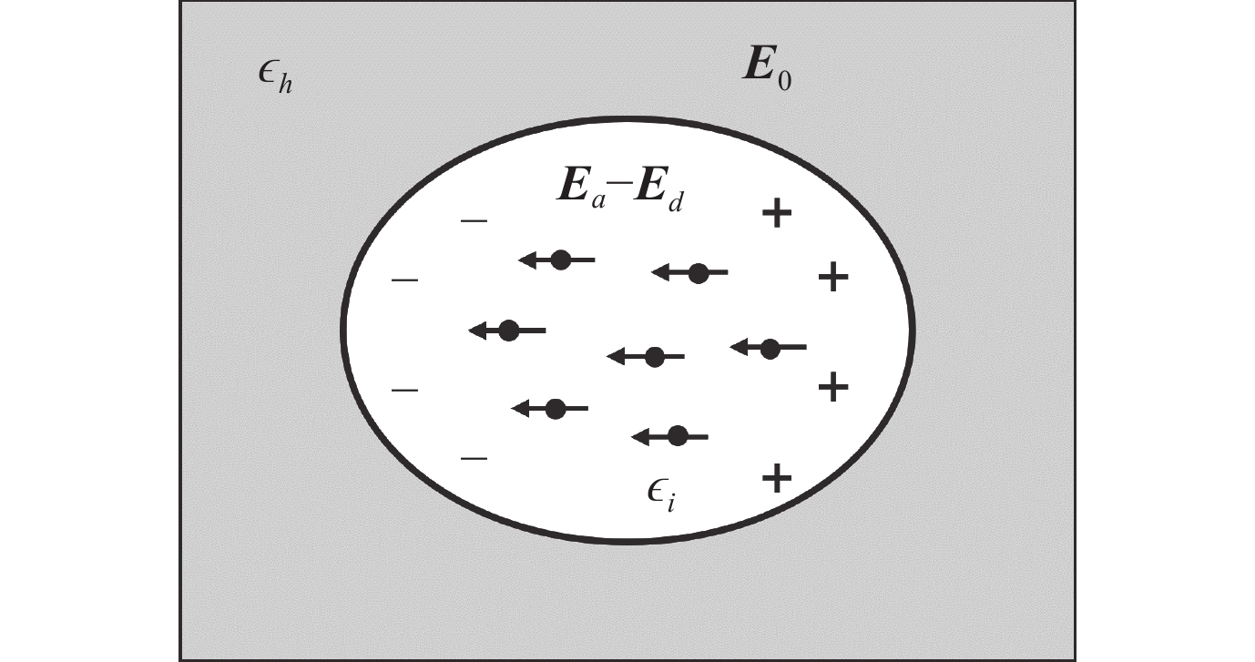


 DownLoad:


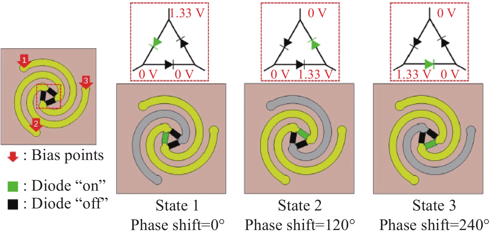


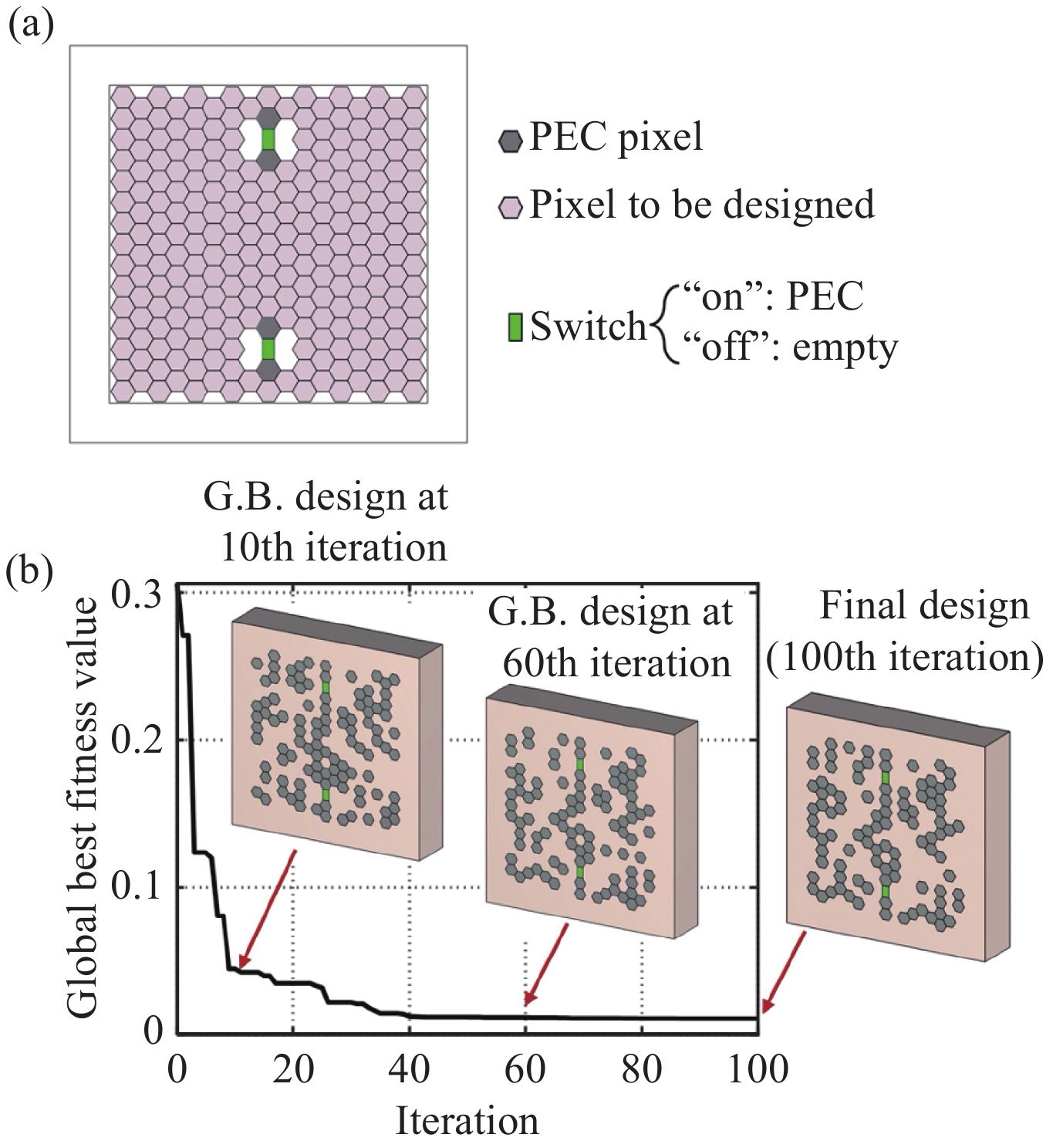


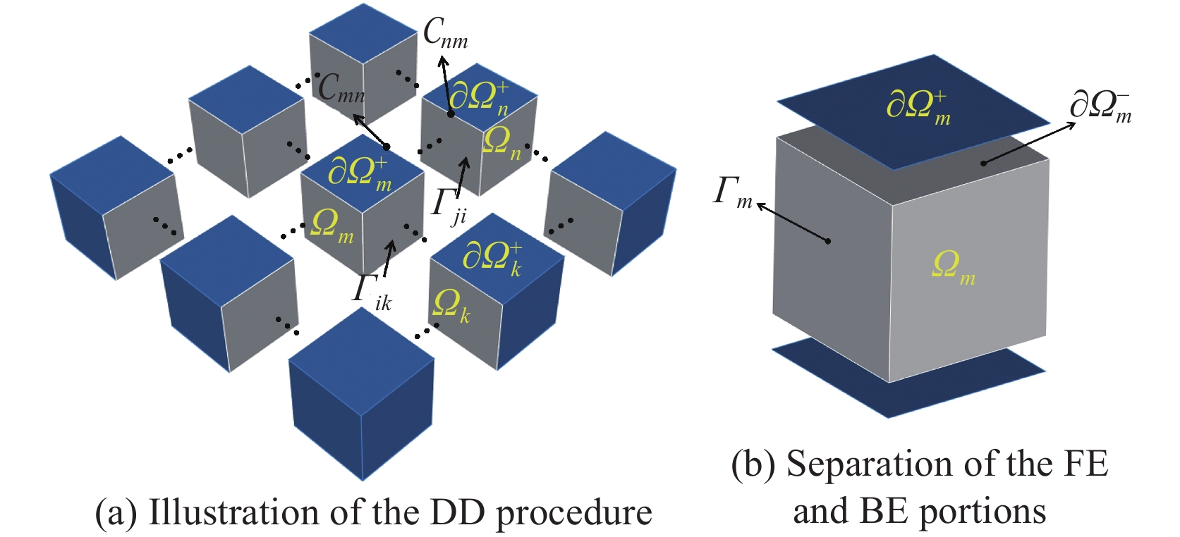
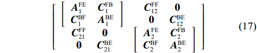


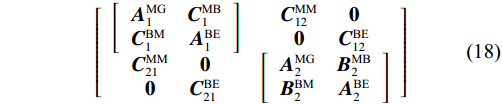


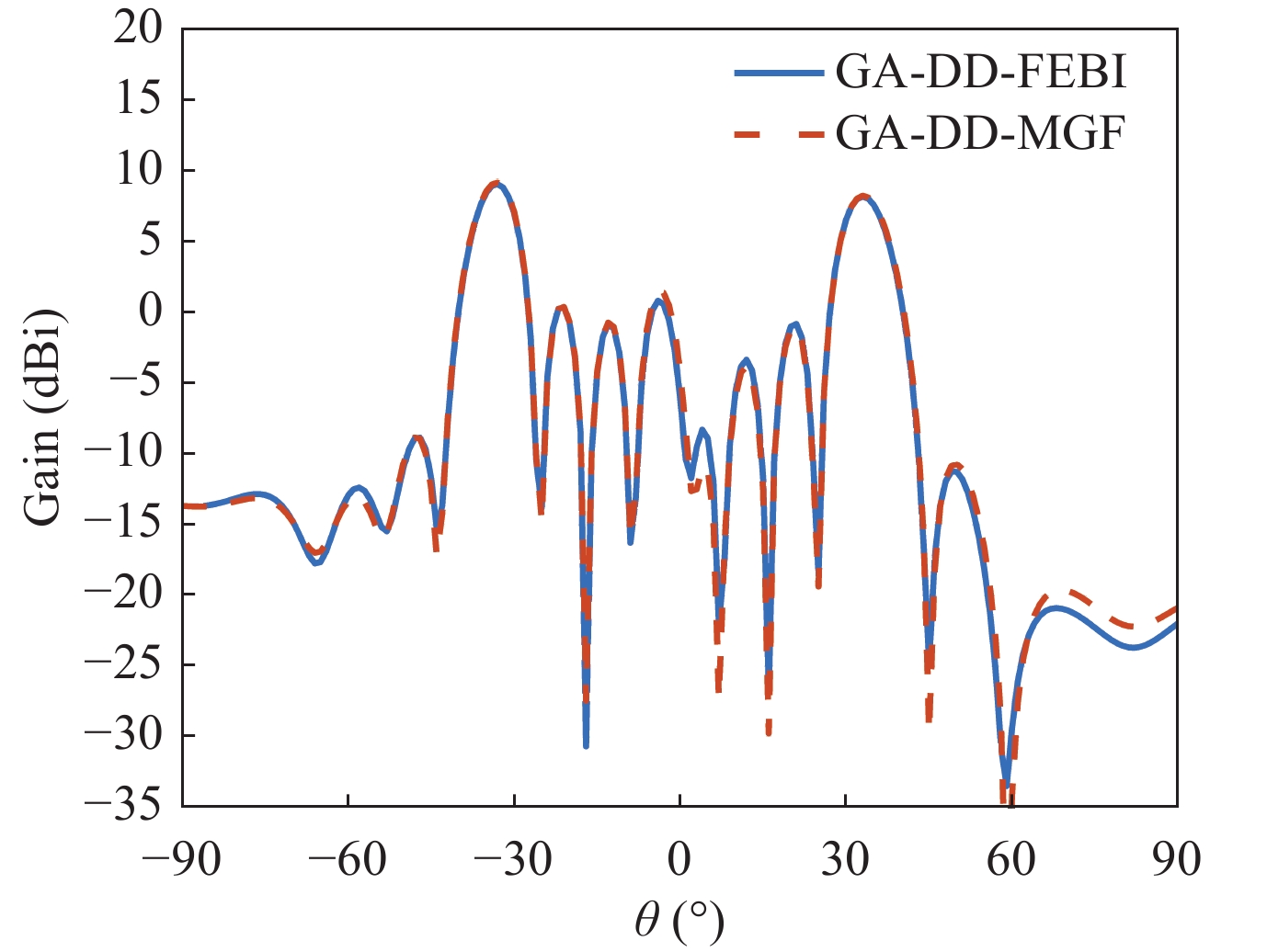


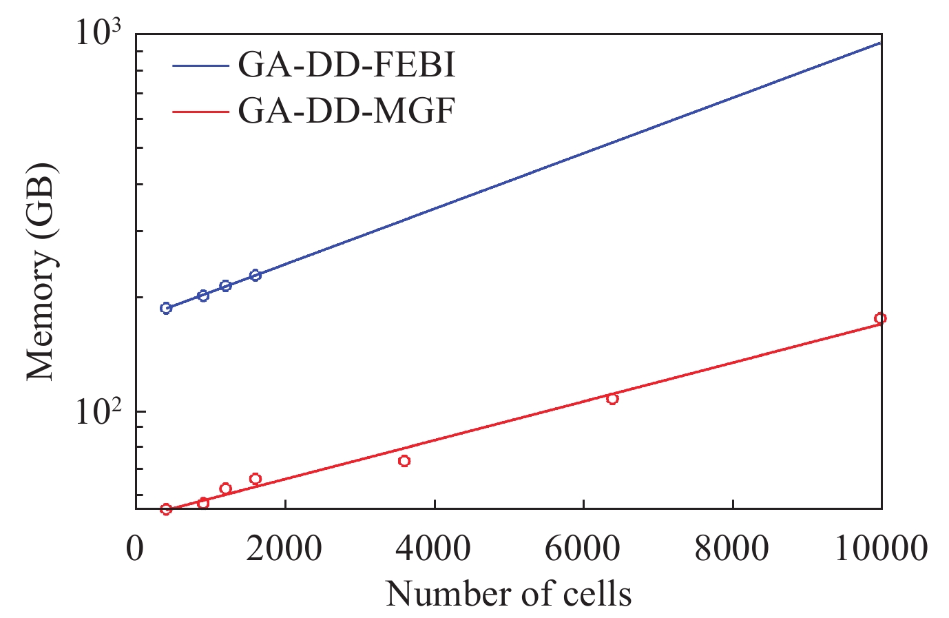
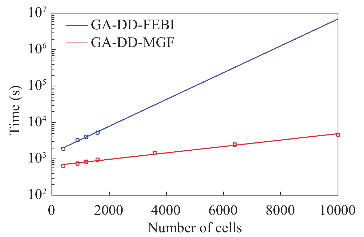
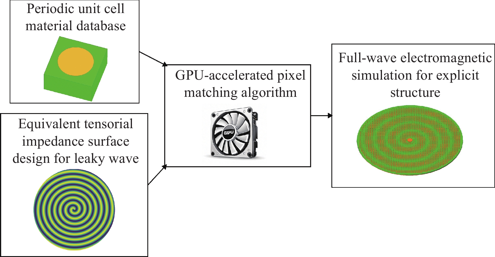


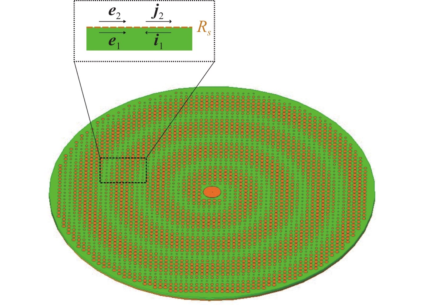


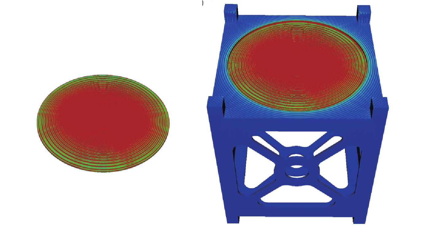
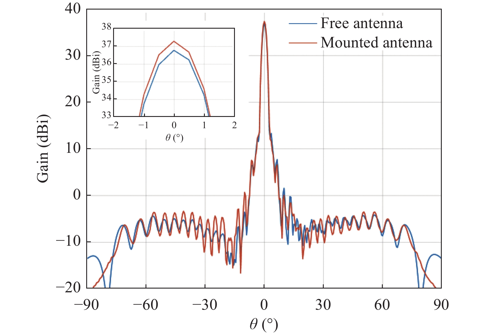
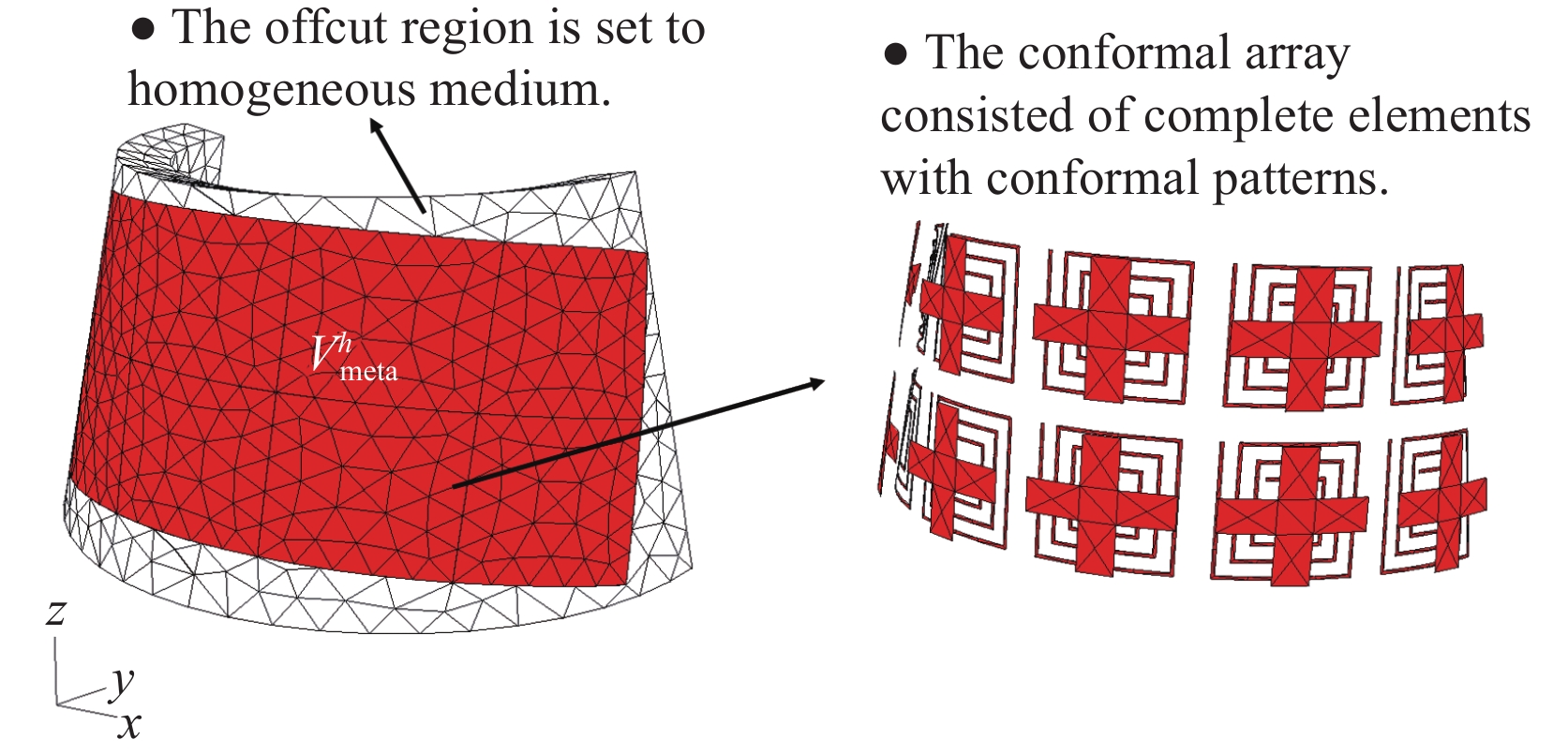


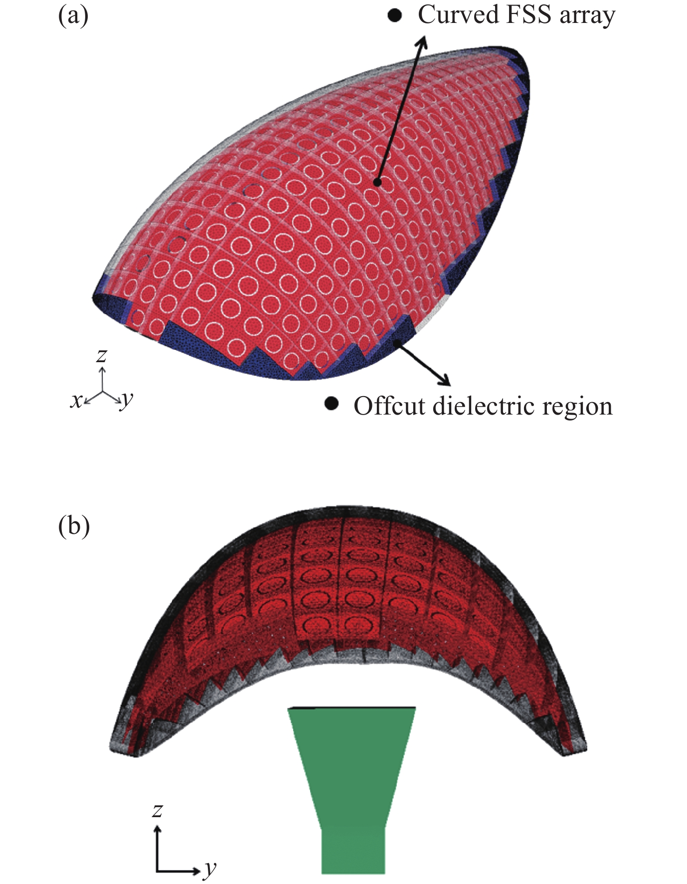
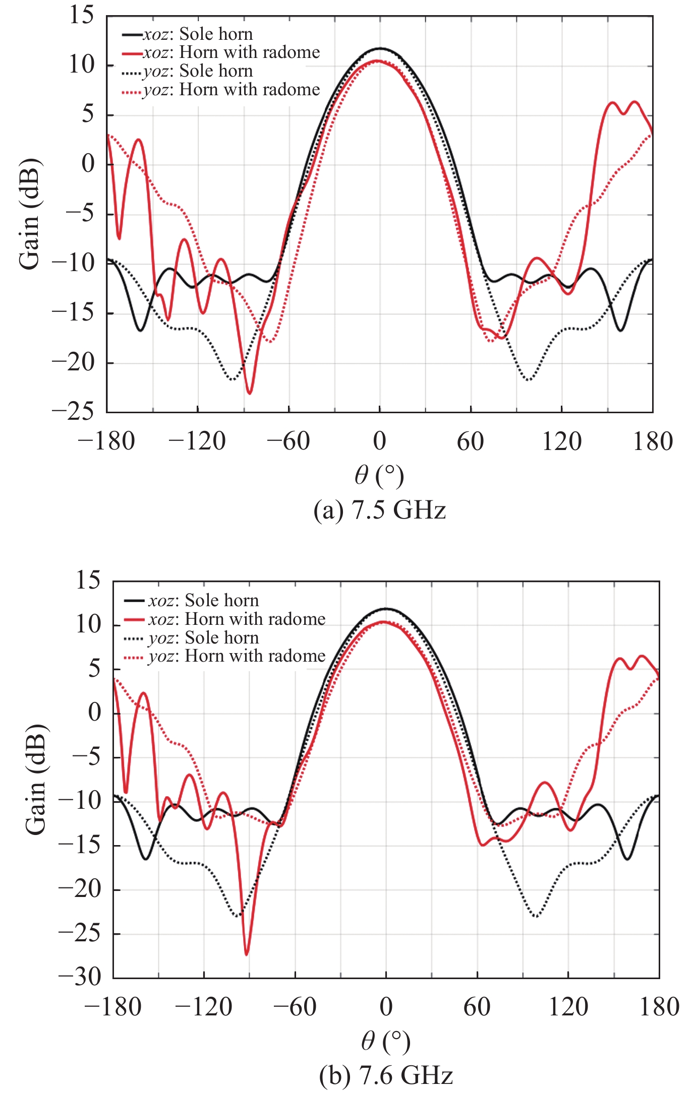


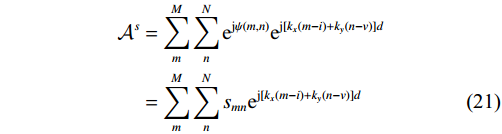
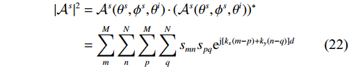


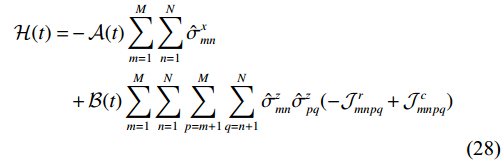


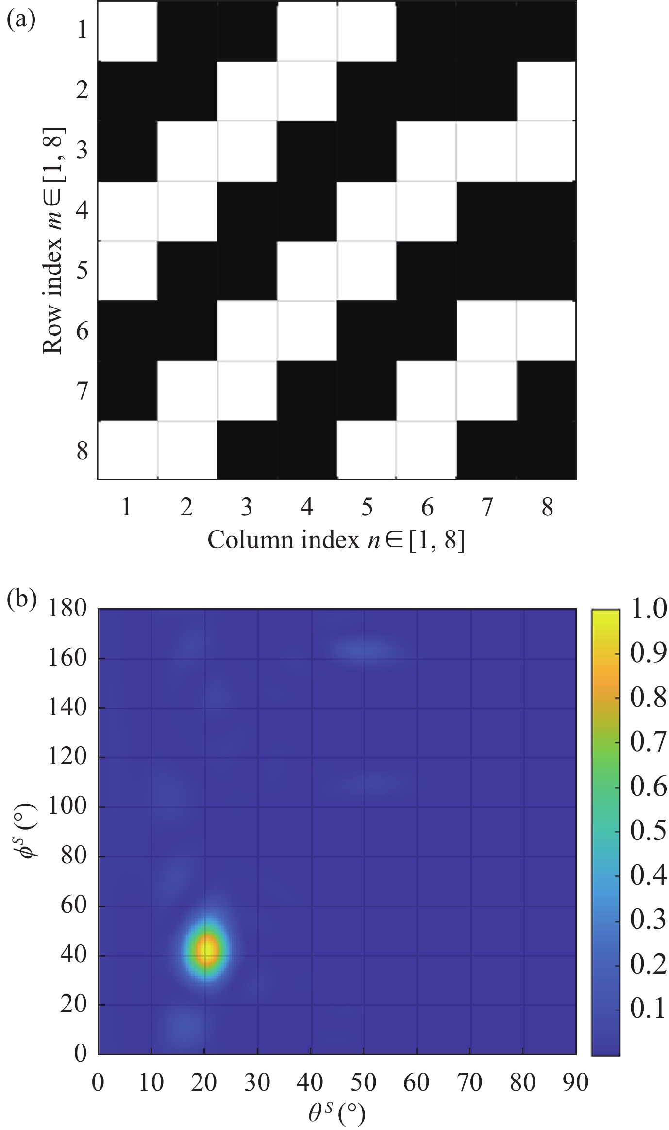


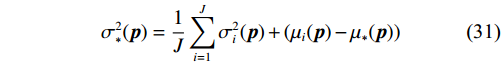


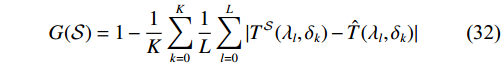


 DownLoad: